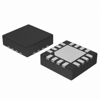
NB7VQ58MMNTXG ON Semiconductor, NB7VQ58MMNTXG Datasheet - Page 5

NB7VQ58MMNTXG
Manufacturer Part Number
NB7VQ58MMNTXG
Description
IC CLOCK/DATA MULTIPLEXER 16QFN
Manufacturer
ON Semiconductor
Series
GigaComm™r
Type
Multiplexer , Datar
Datasheet
1.NB7VQ58MMNTXG.pdf
(9 pages)
Specifications of NB7VQ58MMNTXG
Number Of Circuits
1
Ratio - Input:output
2:1
Differential - Input:output
Yes/Yes
Input
CML, LVDS, LVPECL
Output
CML
Frequency - Max
7GHz
Voltage - Supply
1.71 V ~ 3.6 V
Operating Temperature
-40°C ~ 85°C
Mounting Type
Surface Mount
Package / Case
16-TFQFN Exposed Pad
Frequency-max
7GHz
Lead Free Status / RoHS Status
Lead free / RoHS Compliant
Available stocks
Company
Part Number
Manufacturer
Quantity
Price
Company:
Part Number:
NB7VQ58MMNTXG
Manufacturer:
ON
Quantity:
1 001
NOTE: Device will meet the specifications after thermal equilibrium has been established when mounted in a test socket or printed circuit
11. Measured using a V
12. Input and output voltage swings are single−ended measurements operating in differential mode.
13. Additive RMS jitter with 50% duty cycle clock signal.
14. Additive Peak−to−Peak data dependent jitter with input NRZ data at PRBS23 at 3 Gbps.
15. Crosstalk is measured at the output while applying two similar clock frequencies that are asynchronous with respect to each other at the
Table 7. AC CHARACTERISTICS
f
f
fSEL
V
t
t
t
t
t
t
F
t∫
V
t
Symbol
MAX
DATAMAX
PLH
PHL
PLH
skew
DC
JITTER
r
, t
FN
OUTPP
INPP
N
(20% − 80%).
inputs.
f
,
TC
500
450
400
350
300
250
200
Figure 3. Output Voltage Amplitude (V
board with maintained transverse airflow greater than 500 lfpm. Electrical parameters are guaranteed only over the declared
operating temperature range. Functional operation of the device exceeding these conditions is not implied. Device specification limit
values are applied individually under normal operating conditions and not valid simultaneously.
Frequency (f
0
Maximum Input Clock Frequency
Maximum Operating Data Rate (PRBS23)
Maximum Toggle Frequency, SEL
Output Voltage Amplitude EQEN = 0 or 1
(Note 12) (Figures 3 and 11)
Propagation Delay to Differential Outputs,
@ 1 GHz, measured at differential cross−point EQEN = 0 or 1
Propagation Delay Temperature Coefficient
Device − Device skew (tpdmax – tpdmin)
Output Clock Duty Cycle
(Reference Duty Cycle = 50%)
RMS Random Clock Jitter (Note 13)
Peak−to−Peak Data Dependent Jitter (Note 14)
Phase Noise, f
Integrated Phase Jitter (Figure 4) f
Crosstalk Induced Jitter (Adjacent Channel) (Note 15)
Input Voltage Swing (Differential Configuration) (Figure 11) (Note 12)
Output Rise/Fall Times @ 1 GHz (20% − 80%)
1
f
in
, CLOCK INPUT FREQUENCY (GHz)
2
INPP
in
) at Ambient Temperature (Typical)
3
min source, 50% duty cycle clock source. All output loading with external 50 W to V
c
= 1 GHz
4
5
(V
CC
6
= 1.71 V to 3.6 V; GND = 0 V; T
c
Characteristic
= 1 GHz, 12 kHz − 20 MHz Offset (RMS)
7
OUTPP
8
http://onsemi.com
) vs. Input
9
10
5
−120
−125
−130
−135
−140
−145
−150
−155
−115
A
1.E+03
EQEN = 0 (v 3” FR4)
= −40°C to 85°C) (Note 11)
EQEN = 1 (12” FR4)
V
OUTPP
f
INn/INn to Q, Q
in
f
f
f
in
in
in
v 10.7 Gbps
1.E+04
SEL to Q, Q
(V
v 5.0 GHz
v 7.0 GHz
v 7.0 GHz
f
in
Figure 4. Typical Phase Noise
≥ 200 mV
CC
≤ 7 GHz
100 kHz
10 MHz
20 MHz
40 MHz
10 kHz
1 MHz
FREQUENCY OFFSET (Hz)
= 1.8 V, T = 255C, f
Q, Q
1.E+05
10.7
Min
200
120
100
25
45
40
15
7
5
1.E+06
−135
−136
−150
−151
−151
−151
CC
Typ
400
180
0.2
12
50
13
50
50
50
35
35
8
. Input edge rates 40 ps
c
= 1 GHz)
1200
Max
1.E+07
240
0.8
0.7
22
50
55
60
10
10
50
ps pk−pk
ps RMS
ps rms
Dfs/°C
Gbps
Unit
GHz
MHz
dBc
mV
mV
1.E+08
ps
ns
ps
ps
%
fs


