MC100EP210SFAG ON Semiconductor, MC100EP210SFAG Datasheet

IC DRVR CLK DUAL 1:5 DIFF 32LQFP

MC100EP210SFAG

Manufacturer Part Number
MC100EP210SFAG
Description
IC DRVR CLK DUAL 1:5 DIFF 32LQFP
Manufacturer
ON Semiconductor
Series
100EPr
Type
Fanout Buffer (Distribution)r
Datasheet

Specifications of MC100EP210SFAG

Number Of Circuits
2
Ratio - Input:output
1:5
Differential - Input:output
Yes/Yes
Input
LVDS, LVPECL
Output
LVDS
Frequency - Max
1GHz
Voltage - Supply
2.375 V ~ 2.625 V
Operating Temperature
-40°C ~ 85°C
Mounting Type
Surface Mount
Package / Case
32-LQFP
Frequency-max
1GHz
Number Of Outputs
20
Operating Supply Voltage (max)
2.625V
Operating Temp Range
-40C to 85C
Propagation Delay Time
0.675ns
Operating Supply Voltage (min)
2.375V
Mounting
Surface Mount
Pin Count
32
Operating Supply Voltage (typ)
2.5V
Package Type
LQFP
Input Frequency
>1000MHz
Operating Temperature Classification
Industrial
Max Input Freq
>1000 MHz (Typ)
Propagation Delay (max)
0.65 ns @ 2.375V to 2.625V
Supply Voltage (max)
2.625 V
Supply Voltage (min)
2.375 V
Maximum Operating Temperature
+ 85 C
Minimum Operating Temperature
- 40 C
Mounting Style
SMD/SMT
Lead Free Status / RoHS Status
Lead free / RoHS Compliant
Other names
MC100EP210SFAGOS

Available stocks

Company
Part Number
Manufacturer
Quantity
Price
Part Number:
MC100EP210SFAG
Manufacturer:
ON Semiconductor
Quantity:
10 000
Part Number:
MC100EP210SFAG
Manufacturer:
ON/安森美
Quantity:
20 000
MC100EP210S
2.5V 1:5 Dual Differential
LVDS Compatible Clock
Driver
Description
designed with LVDS clock distribution in mind. The LVDS or
LVPECL input signals are differential and the signal is fanned out to
five identical differential LVDS outputs.
Optimal design, layout, and processing minimize skew within a device
and from device to device.
LVDS inputs, VTA and VTB pins should be unconnected. For
LVPECL inputs, VTA and VTB pins should be connected to the V
(V
distribute low skew LVDS clocks across the backplane or the board.
Features
*For additional information on our Pb−Free strategy and soldering details, please
© Semiconductor Components Industries, LLC, 2006
March, 2006 − Rev. 8
download the ON Semiconductor Soldering and Mounting Techniques
Reference Manual, SOLDERRM/D.
The MC100EP210S is a low skew 1−to−5 dual differential driver,
The EP210S specifically guarantees low output−to−output skew.
Two internal 50 W resistors are provided across the inputs. For
Designers can take advantage of the EP210S performance to
CC
20 ps Typical Output−to−Output Skew
85 ps Typical Device−to−Device Skew
550 ps Typical Propagation Delay
The 100 Series Contains Temperature Compensation
Maximum Frequency > 1 GHz Typical
Operating Range: V
Internal 50 W Input Termination Resistors
LVDS Input/Output Compatible
Pb−Free Packages are Available*
− 2.0 V) supply.
CC
= 2.375 V to 2.625 V with V
EE
= 0 V
1
TT
*For additional marking information, refer to
See detailed ordering and shipping information in the package
dimensions section on page 5 of this data sheet.
Application Note AND8002/D.
CASE 873A
FA SUFFIX
CASE 488AM
LQFP−32
MN SUFFIX
QFN32
ORDERING INFORMATION
1
xxx
A
WL, L
YY, Y
WW, W = Work Week
G
http://onsemi.com
32
= 10 or 100
= Assembly Location
= Wafer Lot
= Year
= Pb−Free Package
Publication Order Number:
1
AWLYYWWG
DIAGRAM*
MARKING
MC100EP210S/D
EP210S
ALYWG
EP210S
MCxxx
MC100

Related parts for MC100EP210SFAG

MC100EP210SFAG Summary of contents

Page 1

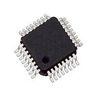
... LVDS Input/Output Compatible • Pb−Free Packages are Available* *For additional information on our Pb−Free strategy and soldering details, please download the ON Semiconductor Soldering and Mounting Techniques Reference Manual, SOLDERRM/D. © Semiconductor Components Industries, LLC, 2006 March, 2006 − Rev. 8 http://onsemi.com LQFP− ...

Page 2

Qa3 Qa3 Qa4 Qa4 Qb0 Qb0 Qa2 27 Qa2 28 Qa1 MC100EP210S 29 Qa1 30 Qa0 31 Qa0 VTA VTB ...

Page 3

Table 2. ATTRIBUTES ESD Protection Moisture Sensitivity, Indefinite Time Out of Drypack (Note 1) Flammability Rating Transistor Count Meets or exceeds JEDEC Spec EIA/JESD78 IC Latchup Test 1. For additional information, refer to Application Note AND8003/D. Table 3. MAXIMUM RATINGS ...

Page 4

Table 4. DC CHARACTERISTICS V Symbol Characteristic I Power Supply Current EE V Output HIGH Voltage (Note Output LOW Voltage (Note Input HIGH Voltage Common Mode IHCMR Range (Differential Configuration) (Note 4) R Internal ...

Page 5

... Driver Device Figure 3. Typical Termination for Output Driver and Device Evaluation ORDERING INFORMATION Device MC100EP210SFA MC100EP210SFAG MC100EP210SFAR2 MC100EP210SFAR2G MC100EP210SMNG MC100EP210SMNR4G †For information on tape and reel specifications, including part orientation and tape sizes, please refer to our Tape and Reel Packaging Specifications Brochure, BRD8011/D. ...

Page 6

−T− DETAIL −Z− −AB− SEATING −AC− PLANE 0.10 (0.004) AC NOTES: 1. DIMENSIONING AND TOLERANCING PER ANSI Y14.5M, 1982. 2. CONTROLLING DIMENSION: MILLIMETER. 3. DATUM PLANE ...

Page 7

... X 0.28 *For additional information on our Pb−Free strategy and soldering details, please download the ON Semiconductor Soldering and Mounting Techniques Reference Manual, SOLDERRM/D. N. American Technical Support: 800−282−9855 Toll Free USA/Canada Japan: ON Semiconductor, Japan Customer Focus Center 2−9−1 Kamimeguro, Meguro−ku, Tokyo, Japan 153−0051 Phone: 81− ...

Related keywords