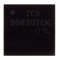
ICS9DB202CK-01LF IDT, Integrated Device Technology Inc, ICS9DB202CK-01LF Datasheet

ICS9DB202CK-01LF
Specifications of ICS9DB202CK-01LF
9DB202CK-01LF
Available stocks
Related parts for ICS9DB202CK-01LF
ICS9DB202CK-01LF Summary of contents
Page 1
... Available in both standard and lead-free RoHS compliant packages • Industrial temperature information available upon request PCIEXT0 VCO nPCIEXC0 1 ICS9DB202- SSIGNMENT IREF DDA CLK 4 21 ICS9DB202-01 nCLK 32-Lead VFQFN 5mm x 5mm x 0.925 package body K Package Top View ICS9DB202CK-01 REV. B FEBRUARY 18, 2009 ...
Page 2
... ICS9DB202-01 PCI EXPRESS JITTER ATTENUATOR ABLE IN ESCRIPTIONS ABLE IN HARACTERISTICS IDT ™ / ICS ™ PCI EXPRESS JITTER ATTENUATOR Ω Ω ICS9DB202CK-01 REV. B FEBRUARY 18, 2009 KΩ KΩ ...
Page 3
... Exposure to absolute maximum rating conditions for ex- tended periods may affect product reliability 3.3V±5 0° 3.3V±5 0°C 70°C, RREF = 475Ω 3.3V±5 0°C 70°C, RREF = 475Ω 0°C 70°C, RREF = 475Ω 70°C, RREF = 475Ω ICS9DB202CK-01 REV. B FEBRUARY 18, 2009 µ A µ µ ...
Page 4
... PLL, it will increase the output phase noise performance of the device recommended that the phase noise performance of the input is verified in order to achieve the above phase noise performance PCI Express™ Filter 100MHz RMS Phase Jitter (Random) 1.5MHz to 22MHz = 2.31ps 1M 10M ( ICS9DB202CK-01 REV. B FEBRUARY 18, 2009 100M ...
Page 5
... PCI EXPRESS JITTER ATTENUATOR M EASUREMENT SCOPE nCLK GND C D IRCUIT IFFERENTIAL PCIEXC0 PCIEXT0 ➤ tcycle n+1 O UTPUT 80 20 NFORMATION Cross Points PP CLK I L NPUT EVEL PERIOD t PW odc = x 100% t PERIOD UTY YCLE ULSE IDTH ERIOD ICS9DB202CK-01 REV. B FEBRUARY 18, 2009 V CMR ...
Page 6
... V and R2/R1 = 0.609. VDD R1 1K Single Ended Clock Input V_REF C1 0. INGLE NDED IGNAL RIVING 6 3. .01μF 24Ω V DDA .01μF 10μ IGURE OWER UPPLY ILTERING = 3.3V, V_REF should be 1.25V DD CLK nCLK D I IFFERENTIAL NPUT ICS9DB202CK-01 REV. B FEBRUARY 18, 2009 ...
Page 7
... Ohm 3D CLK/nCLK LOCK NPUT D 3.3V LVDS D RIVEN BY A RIVER 2. 120 120 Zo = 60Ω 60Ω SSTL R1 R2 120 120 3F CLK/nCLK LOCK NPUT D 2.5V SSTL D RIVEN BY A RIVER ICS9DB202CK-01 REV. B FEBRUARY 18, 2009 HiPerClockS Input 3.3V CLK nCLK Receiv er 3.3V CLK nCLK HiPerClockS ...
Page 8
... Note on the Surface Mount Assembly of Amkor’s Thermally/ Electrically Enhance Leadframe Base Package, Amkor Technology. EXPOSED HEAT SLUG THERMAL VIA XPOSED AD HERMAL ELEASE ATH 8 SOLDER PIN LAND PATTERN PIN PAD (GROUND PAD) – IDE IEW RAWING NOT TO CALE ICS9DB202CK-01 REV. B FEBRUARY 18, 2009 ...
Page 9
... IDT ™ / ICS ™ PCI EXPRESS JITTER ATTENUATOR termination, which has a slightly better signal integrity, is recommended for all other applications. VDD IREF VDDA CLK nCLK VDD 9DB202-01_lqf p32_short ICS9DB202-01 IGURE XAMPLE TL1 HCSL TL2 ICS9DB202CK-01 REV. B FEBRUARY 18, 2009 ...
Page 10
... IDT ™ / ICS ™ PCI EXPRESS JITTER ATTENUATOR F 6A IGURE ECOMMENDED ERMINATION and receiver on the same PCB. All traces should all be 50Ω impedance IGURE ECOMMENDED ERMINATION 10 ICS9DB202CK-01 REV. B FEBRUARY 18, 2009 ...
Page 11
... OWER ONSIDERATIONS = 3. 3.465V, which gives worst case results 3.465V * (112mA + 22mA) = 464.3mW DDA_MAX TM devices is 125°C. * Pd_total + 32-P VFQFN ORCED ONVECTION θ θ θ θ θ 0 Air Flow (Linear Feet per Minute 34.8C/W 11 must be used. Assuming no air JA ICS9DB202CK-01 REV. B FEBRUARY 18, 2009 ...
Page 12
... I DD_MAX L OUT OUT = (3.465V – 17mA * 50Ω) * 17mA Total Power Dissipation per output pair = 44.5mW IDT ™ / ICS ™ PCI EXPRESS JITTER ATTENUATOR OUT = 17mA HCSL D C IGURE RIVER IRCUIT AND DD_MAX OUT R L 50Ω T ERMINATION ICS9DB202CK-01 REV. B FEBRUARY 18, 2009 ...
Page 13
... Multi-Layer PCB, JEDEC Standard Test Boards T C RANSISTOR OUNT The transistor count for ICS9DB202-01 is: 2471 IDT ™ / ICS ™ PCI EXPRESS JITTER ATTENUATOR R I ELIABILITY NFORMATION 32 L VFQFN P EAD ACKAGE 0 Air Flow (Linear Feet per Minute 34.8C/W 13 ICS9DB202CK-01 REV. B FEBRUARY 18, 2009 ...
Page 14
... IDT ™ / ICS ™ PCI EXPRESS JITTER ATTENUATOR VFQFN EAD this device. The pin count and pinout are shown on the front page. The package dimensions are in Table 8 below ABLE ACKAGE IMENSIONS Reference Document: JEDEC Publication 95, MO-220 ICS9DB202CK-01 REV. B FEBRUARY 18, 2009 ...
Page 15
... IDT does not authorize or warrant any IDT product for use in life support devices or critical medical instruments. IDT ™ / ICS ™ PCI EXPRESS JITTER ATTENUATOR " " " " " " ° & ° ° & ° ICS9DB202CK-01 REV. B FEBRUARY 18, 2009 ° ° ° ° ...
Page 16
... ICS9DB202-01 PCI EXPRESS JITTER ATTENUATOR IDT ™ / ICS ™ PCI EXPRESS JITTER ATTENUATOR " " ICS9DB202CK-01 REV. B FEBRUARY 18, 2009 ...
Page 17
ICS9DB202-01 PCI EXPRESS JITTER ATTENUATOR Innovate with IDT and accelerate your future networks. Contact: www.IDT.com For Sales 800-345-7015 (inside USA) +408-284-8200 (outside USA) Fax: 408-284-2775 www.IDT.com/go/contactIDT © 2009 Integrated Device Technology, Inc. All rights reserved. Product specifications subject to change ...


