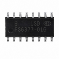
FS6377-01G-XTD ON Semiconductor, FS6377-01G-XTD Datasheet - Page 6

FS6377-01G-XTD
Manufacturer Part Number
FS6377-01G-XTD
Description
IC CLOCK GEN 3-PLL PROGR 16-SOIC
Manufacturer
ON Semiconductor
Type
PLL Clock Generatorr
Datasheet
1.FS6377-01G-XTD.pdf
(24 pages)
Specifications of FS6377-01G-XTD
Pll
Yes
Input
Crystal
Output
CMOS
Number Of Circuits
1
Ratio - Input:output
1:4
Differential - Input:output
No/No
Frequency - Max
230MHz
Divider/multiplier
Yes/No
Voltage - Supply
3 V ~ 5.5 V
Operating Temperature
0°C ~ 70°C
Mounting Type
Surface Mount
Package / Case
16-SOIC (3.9mm Width)
Frequency-max
230MHz
Mounting Style
SMD/SMT
Number Of Outputs
1
Operating Temperature Range
0 C to + 70 C
Supply Current
43 mA
Lead Free Status / RoHS Status
Lead free / RoHS Compliant
Other names
766-1026
Available stocks
Company
Part Number
Manufacturer
Quantity
Price
Company:
Part Number:
FS6377-01G-XTD
Manufacturer:
ON Semiconductor
Quantity:
45
FS6377
4.3 Oscillator Overdrive
For applications where an external reference clock is provided (and the crystal oscillator is not required), the reference clock should be
connected to XOUT and XIN should be left unconnected (float).
For best results, make sure the reference clock signal is as jitter-free as possible, can drive a 40pF load with fast rise and fall times and
can swing rail-to-rail.
If the reference clock is not a rail-to-rail signal, the reference must be AC coupled to XOUT through a 0.01µF or 0.1µF capacitor. A
minimum 1V peak-to-peak signal is required to drive the internal differential oscillator buffer.
2
5.0 I
C-bus Control Interface
2
This device is a read/write slave device meeting all Philips I
C-bus specifications except a "general call." The bus has to be controlled
by a master device that generates the serial clock SCL, controls bus access and generates the START and STOP conditions while the
device works as a slave. Both master and slave can operate as a transmitter or receiver, but the master device determines which mode
is activated. A device that sends data onto the bus is defined as the transmitter, and a device receiving data as the receiver.
2
I
C-bus logic levels noted herein are based on a percentage of the power supply (V
). A logic-one corresponds to a nominal voltage of
DD
VDD, while a logic-zero corresponds to ground (V
).
SS
5.1 Bus Conditions
Data transfer on the bus can only be initiated when the bus is not busy. During the data transfer, the data line (SDA) must remain stable
whenever the clock line (SCL) is high. Changes in the data line while the clock line is high will be interpreted by the device as a START
2
or STOP condition. The following bus conditions are defined by the I
C-bus protocol.
5.1.1. Not Busy
Both the data (SDA) and clock (SLC) lines remain high to indicate the bus is not busy.
5.1.2. START Data Transfer
A high to low transition of the SDA line while the SCL input is high indicates a START condition. All commands to the device must be
preceded by a START condition.
5.1.3. STOP Data Transfer
A low to high transition of the SDA line while SCL is held high indicates a STOP condition. All commands to the device must be
followed by a STOP condition.
5.1.4. Data Valid
The state of the SDA line represents valid data if the SDA line is stable for the duration of the high period of the SCL line after a START
condition occurs. The data on the SDA line must be changed only during the low period of the SCL signal. There is one clock pulse per
data bit.
Each data transfer is initiated by a START condition and terminated with a STOP condition. The number of data bytes transferred
between START and STOP conditions is determined by the master device, and can continue indefinitely. However, data that is
overwritten to the device after the first sixteen bytes will overflow into the first register, then the second, and so on, in a first-in, first-
overwritten fashion.
Rev. 4 | Page 6 of 24 | www.onsemi.com


