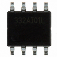
ICS87332AMI-01LF IDT, Integrated Device Technology Inc, ICS87332AMI-01LF Datasheet - Page 9

ICS87332AMI-01LF
Manufacturer Part Number
ICS87332AMI-01LF
Description
IC CLK GEN /2 ECL/LVPECL 8-SOIC
Manufacturer
IDT, Integrated Device Technology Inc
Series
HiPerClockS™r
Type
Clock Generatorr
Datasheet
1.ICS87332AMI-01LF.pdf
(14 pages)
Specifications of ICS87332AMI-01LF
Pll
No
Input
HCSL, LVDS, LVHSTL, LVPECL, SSTL
Output
ECL, LVPECL
Number Of Circuits
1
Ratio - Input:output
1:1
Differential - Input:output
Yes/Yes
Frequency - Max
500MHz
Divider/multiplier
Yes/No
Voltage - Supply
2.375 V ~ 3.8 V
Operating Temperature
-40°C ~ 85°C
Mounting Type
Surface Mount
Package / Case
8-SOIC
Frequency-max
500MHz
Number Of Outputs
2
Operating Supply Voltage (max)
-3.8/3.8V
Operating Temp Range
-40C to 85C
Propagation Delay Time
1.6ns
Operating Supply Voltage (min)
-2.375/2.375V
Mounting
Surface Mount
Pin Count
8
Operating Supply Voltage (typ)
-2.5/-3.3/3.3V
Package Type
SOIC N
Input Frequency
1GHz
Duty Cycle
51%
Operating Temperature Classification
Industrial
Lead Free Status / RoHS Status
Lead free / RoHS Compliant
Other names
800-1204
800-1204-5
800-1204
87332AMI-01LF
800-1204-5
800-1204
87332AMI-01LF
Available stocks
Company
Part Number
Manufacturer
Quantity
Price
Company:
Part Number:
ICS87332AMI-01LF
Manufacturer:
IDT Integrated Device Technolo
Quantity:
135
This section provides information on power dissipation and junction temperature for the ICS87332I-01.
Equations and example calculations are also provided.
1. Power Dissipation.
The total power dissipation for the ICS87332I-01 is the sum of the core power plus the power dissipated in the load(s).
The following is the power dissipation for V
NOTE: Please refer to Section 3 for details on calculating power dissipated in the load.
2. Junction Temperature.
Junction temperature at the junction of the bond wire and bond pad directly affects the reliability of the device. The maximum
recommended junction temperature for HiPerClockS
125°C ensures that the bond wire and bond pad temperature remains below 125°C.
In order to calculate junction temperature, the appropriate junction-to-ambient thermal resistance
moderate air flow of 200 linear feet per minute and a multi-layer board, the appropriate value is 103.3°C/W per Table 5 below.
Therefore, Tj for an ambient temperature of 85°C with all outputs switching is:
This calculation is only an example. Tj will obviously vary depending on the number of loaded outputs, supply voltage, air flow,
and the type of board (multi-layer).
T
ICS87332I-01 Data Sheet
ICS87332AMI-01 REVISION C NOVEMBER 16, 2009
ABLE
5. T
Power (core)
Power (outputs)
Total Power
The equation for Tj is as follows: Tj =
Tj = Junction Temperature
Pd_total = Total Device Power Dissipation (example calculation is in section 1 above)
T
85°C + 0.144W * 103.3°C/W = 99.9°C. This is well below the limit of 125°C
JA
A
Single-Layer PCB, JEDEC Standard Test Boards
Multi-Layer PCB, JEDEC Standard Test Boards
NOTE: Most modern PCB designs use multi-layered boards. The data in the second row pertains to most designs.
= Ambient Temperature
HERMAL
= Junction-to-Ambient Thermal Resistance
R
MAX
ESISTANCE
_MAX
MAX
= V
(3.8V, with all outputs switching) = 114mW + 30mW = 144mW
= 30mW/Loaded Output pair
CC_MAX
JA
* I
EE_MAX
FOR
8-
CC
= 3.8V * 30mA = 114mW
JA
PIN
= 3.8V, which gives worst case results.
P
by Velocity (Linear Feet per Minute)
JA
SOIC, F
OWER
* Pd_total + T
TM
devices is 125°C. Limiting the internal transistor junction temperature, Tj, to
ORCED
C
A
ONSIDERATIONS
C
ONVECTION
9
153.3°C/W
112.7°C/W
0
÷2DIFFERENTIAL-TO-2.5V/3.3V ECL/LVPECL CLOCK GENERATOR
128.5°C/W
103.3°C/W
200
JA
must be used . Assuming a
2009 Integrated Device Technology, Inc.
115.5°C/W
97.1°C/W
500


