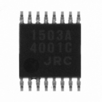
NJW1503AV-TE1# NJR, NJW1503AV-TE1# Datasheet

NJW1503AV-TE1#
Specifications of NJW1503AV-TE1#
NJW#1503AV-TE1
Available stocks
Related parts for NJW1503AV-TE1#
NJW1503AV-TE1# Summary of contents
Page 1
... BAND SW 4bit HF IN PreAMP CP VCC2 AMPOUT AMP VCC3 4bit Latch Programmable 1/8 Divider 15bit Phase Phase OUT Comp NJW1503A PACKAGE OUTLINE NJW1503AV VCC1 5V GND CS 3Wire Bus DAT Receiver CLK 15bit Latch 8bit Latch OSCOUT 1/1024 X’tal 1/512 XTAL OSC (1/640) Ref ...
Page 2
NJW1503A ABSOLUTE MAXIMUM RATINGS Parameter Supply Voltage (Vcc1,3) Supply Voltage (Vcc2) Input Voltage(except 3-wire bus) Output Voltage (except 3-wire bus) 3-Wire bus Input Voltage Power Dissipation Operating Temperature Range Storage Temperature Range RECOMMENDED OPERATING CONDITION Parameter Operating Voltage Vcc1,Vcc3 Operating ...
Page 3
ELECTRICAL CHARACTERISTICS Parameter Operating Current Operating Current 2 AMPOUT: Low Level AMP Input Current Phase OUT :High Imp (2.5V) ANP OUT : Low Level AMP Output Current AMP OUT Input=5V AMP Gain f=1KHz Phase Comparator Current Source ...
Page 4
NJW1503A TEST CIRCUIT CS 18p 100 4MHz -20dBm - 4 - DAT CLK 100 100 VS3 VS2 2mV 5V 2.5V 1kHz 34V 270 316k 11 10 ...
Page 5
Serial Bus Data Format (3-Wire bus) 1. Bus protocol for18bit N13 N12 N11 N10 Reference divider : f xtal 2. Bus protocol for19bit ...
Page 6
NJW1503A TERMINAL CHARACTERISTICS Typ.DC No. Symbol Voltage ( 3.2 2 GND 0 3 VCC1 5 4 VCC3 5 5 BS3 0 6 BS2 7 BS1 0 8 BS0 Equivalent Circuit 1 3 ...
Page 7
Typ.DC No. Symbol Voltage (V) 10 AMPOUT - 11 VCC2 32 12 OSCOUT 4.1 13 CLK - 14 DAT - XTAL 3.3 Equivalent Circuit NJW1503A Function Amplifier Output Amplifier ...
Page 8
NJW1503A TYPICAL CHARACTERISTICS VCC1 Supply Current Curve 40.0 35.0 30.0 25.0 20.0 15.0 10.0 5.0 0.0 0.0 1.0 2.0 3.0 4.0 VCC1 Supply Voltage BS0-BS2 Output Current Curve 50.0 40.0 30.0 20.0 10.0 0.0 3.0 3.5 4.0 Output Voltage - ...
Page 9
MEMO [CAUTION] The specifications on this databook are only given for information , without any guarantee as regards either mistakes or omissions. The application circuits in this databook are described only to show representative usages of the product and not ...


