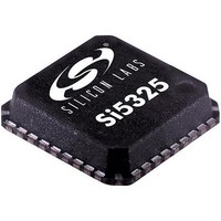
SI5325B-C-GM Silicon Laboratories Inc, SI5325B-C-GM Datasheet - Page 51

SI5325B-C-GM
Manufacturer Part Number
SI5325B-C-GM
Description
IC UP-PROG CLK MULTIPLIER 36-QFN
Manufacturer
Silicon Laboratories Inc
Type
Clock Multiplierr
Datasheet
1.SI5325C-C-GM.pdf
(52 pages)
Specifications of SI5325B-C-GM
Number Of Circuits
1
Package / Case
36-QFN
Pll
Yes
Input
Clock
Output
CML, CMOS, LVDS, LVPECL
Ratio - Input:output
2:2
Differential - Input:output
Yes/Yes
Frequency - Max
808MHz
Divider/multiplier
Yes/Yes
Voltage - Supply
1.71 V ~ 3.63 V
Operating Temperature
-40°C ~ 85°C
Mounting Type
Surface Mount
Frequency-max
808MHz
Maximum Input Frequency
710 MHz
Minimum Input Frequency
10 MHz
Output Frequency Range
10 MHz to 808 MHz
Supply Voltage (max)
3.63 V
Supply Voltage (min)
1.71 V
Maximum Operating Temperature
+ 85 C
Minimum Operating Temperature
- 40 C
Mounting Style
SMD/SMT
Operating Supply Voltage
1.8 V, 2.5 V, 3.3 V
Lead Free Status / RoHS Status
Lead free / RoHS Compliant
Si5325
D
Revision 0.23 to Revision 0.24
Revision 0.24 to Revision 0.25
Revision 0.25 to Revision 0.26
Revision 0.26 to Revision 0.3
Revision 0.3 to Revision 0.4
51
OCUMENT
Clarified that the two outputs have a common, higher
frequency source on page 1.
Changed LVTTL to LVCMOS in Table 2, “Absolute
Maximum Ratings,” on page 5.
Added Figure 1, “Typical Phase Noise Plot,” on page
4.
Updated “2. Pin Descriptions: Si5325”.
Updated "5. Ordering Guide" on page 47.
Added “7. Recommended PCB Layout”.
Updated Section "2. Pin Descriptions: Si5325" on
page 9.
Removed Figure 1. “Typical Phase Noise Plot.”
Changed pins 11 and 15 from NC to VDD in “2. Pin
Descriptions: Si5325”.
Changed 1.8 V operating range to ±5%.
Updated Table 1 on page 4.
Updated Table 2 on page 5.
Added page 6.
Updated "1. Functional Description" on page 8.
Clarified "2. Pin Descriptions: Si5325" on page 9
including pull-up/pull-down.
Added register map
Lowered minimum CKOUT frequency
Updated spec tables
Added to spec table
No bypass mode with CMOS outputs
Removed references to latency control, INC, and DEC.
Changed font for register names to underlined italics.
ESD tolerance, Table 2 on page 5
Minimum input and output clock frequencies, Table 1 on
page 4
Absolute maximum VDD voltage, Table 2 on page 5
CKIN voltage limits, Table 2 on page 5
Typical jitter and phase noise values, Table 1 on page 4
C
HANGE
L
IST
Preliminary Rev. 0.4


