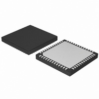
NB7N017MMNR2G ON Semiconductor, NB7N017MMNR2G Datasheet

NB7N017MMNR2G
Specifications of NB7N017MMNR2G
Available stocks
Related parts for NB7N017MMNR2G
NB7N017MMNR2G Summary of contents
Page 1
NB7N017M 3.3V SiGe 8−Bit Dual Modulus Programmable Divider/Prescaler with CML Outputs The NB7N017M is a high speed 8–bit dual modulus programmable divider/prescaler with 16 mA CML outputs capable of switching at input frequencies greater than 3.5 GHz. The CML output ...
Page 2
NB7N017M PLa 2 Pa0 3 Pa1 4 5 Pa2 NB7N017M 7 Pa3 Pa4 Pa5 10 Pa6 11 12 Pa7 13 NC Figure 1. Pinout (Top View) http://onsemi.com ...
Page 3
Table 1. PIN DESCRIPTION Pin Name I/O CLK ECL, CML, LVCMOS, LVDS, LVTTL Input CE ECL, CML, LVCMOS, LVDS, LVTTL Input MR CMOS, ECL Input SEL ECL, CML, LVCMOS, LVDS, LVTTL Input PLa, PLb CMOS, ECL Input TC CML Output ...
Page 4
Table 2. CE Truth Table CE Clock Status LOW Clock Disabled HIGH Clock Enabled Table 4. Register Programming Values for Various Divide Ratios Pa7/Pb7 Pa6/Pb6 Pa5/Pb5 Pa4/Pb4 − ...
Page 5
CLK CLK = VTCLK VTCLK = INTERNAL D INTERNAL NB7N017M Figure 2. Input Structure ...
Page 6
CLK CLK_INT CLK CLK_INT GENERATOR CE 8−BIT CE COUNTER MR SEL TCLD MUX SEL Pa_INT[7:0] 8−BIT REGa PLa Pa[7:0] Table 6. Interface Options CLK INPUT interfacing options CML LVDS AC−COUPLED RSECL, PECL, NECL LVTTL, LVCMOS Table 7. ATTRIBUTES Characteristic Internal ...
Page 7
Table 8. MAXIMUM RATINGS Symbol Parameter V Positive Power Supply CC V Negative Power Supply EE V Positive Input I Negative Input V Differential Input Voltage INPP (50 W Resistor) I Input Current through Output Current ...
Page 8
Table 9. DC CHARACTERISTICS, POSITIVE CML OUTPUT Symbol Characteristic I Positive Power Supply Current CC V Output HIGH Voltage (Note 12 Output LOW Voltage (Note 12) OL DIFFERENTIAL INPUT DRIVEN SINGLE−ENDED (Figures 19, 21) V Input Threshold Reference ...
Page 9
Table 10. DC CHARACTERISTICS, NEGATIVE CML OUTPUT Symbol Characteristic I Positive Power Supply Current CC V Output HIGH Voltage (Note 17 Output LOW Voltage OL (Note 17) DIFFERENTIAL INPUT DRIVEN SINGLE−ENDED (Figures 19, 21) V Input Threshold Reference ...
Page 10
Table 11. AC CHARACTERISTICS V Symbol Characteristic Output Voltage Amplitude @ B 2 Mode V OUTPP (See Figure Propagation Delay to Output Differential PLH t PHL t RMS Random Clock Jitter f = 3.5 GHz JITTER in ...
Page 11
Application Information All NB7N017M inputs can accept PECL, CML, LVTTL, LVCMOS and LVDS signal levels. The limitations for differential input signal (LVDS, PECL, or CML) are PECL Driver Recommended R Values ...
Page 12
V CC LVTTL/ LVCMOS Driver V EE Figure 9. LVCMOS/LVTTL to CML Receiver Interface Table 12. OPERATION TABLE MR Pa PLa 1 XXXXXXXX x XXXXXXXX 0 00000101 H 0 00000101 H 0 XXXXXXXX L XXXXXXXX 0 XXXXXXXX L XXXXXXXX 0 ...
Page 13
Table 12. OPERATION TABLE MR Pa PLa 0 XXXXXXXX L XXXXXXXX 0 XXXXXXXX L XXXXXXXX 0 XXXXXXXX L XXXXXXXX 0 XXXXXXXX L XXXXXXXX 0 XXXXXXXX L XXXXXXXX 0 XXXXXXXX L XXXXXXXX 0 XXXXXXXX L XXXXXXXX 0 XXXXXXXX L XXXXXXXX 0 ...
Page 14
NB7N017M MR Pa[7:0] 05 PLa Pa_INT[7:0] Pb[7:0] 04 PLb Pb_INT[7:0] SEL CE CLK CLK_INT TC_INT TC Figure 10. Device Timing Diagram for Table 12 MR CLK CE CLK_INT Figure 11. Timing Diagram for CE Input http://onsemi.com ...
Page 15
NB7N017M MR delay CLK PLa Pa[7:0] 0B d=12 d=12 TC[7:0] Figure 12. Timing Diagram for PLa / PLb Inputs (SEL is Low) MR delay CLK PLa Pa[7:0] d=12 d=256 d=256 TC[7:0] Figure 13. Timing Diagram for PLa / PLb Inputs ...
Page 16
NB7N017M MR CLK SEL Pa[7:0] Pb[7:0] PLa PLb d=4 d=4 TC[7:0] Figure 15. Timing Diagram for SEL Input (Before Critical Rising Edge of CLK) MR CLK SEL Pa[7:0] Pb[7:0] PLa PLb d=4 d=4 TC[7:0] Figure 16. Timing Diagram for SEL ...
Page 17
CLK CLK Figure 19. Differential Input Driven Single−Ended thmax IHmax V ILmax IHmin V thmin V ILmin GND Figure ...
Page 18
... Q Q Figure 24. Typical Termination for 16 mA Output Drive and Device Evaluation ORDERING INFORMATION Device NB7N017MMN NB7N017MMNG NB7N017MMNR2 NB7N017MMNR2G †For information on tape and reel specifications, including part orientation and tape sizes, please refer to our Tape and Reel Packaging Specifications Brochure, BRD8011/D. NB7N017M + Figure 23 ...
Page 19
... NOTE American Technical Support: 800−282−9855 Toll Free USA/Canada Japan: ON Semiconductor, Japan Customer Focus Center 2−9−1 Kamimeguro, Meguro−ku, Tokyo, Japan 153−0051 Phone: 81−3−5773−3850 http://onsemi.com 19 NOTES: 1. DIMENSIONING AND TOLERANCING PER ASME Y14.5M, 1994. 2. CONTROLLING DIMENSION: MILLIMETERS 3 ...


