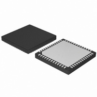
NB7N017MMNR2G ON Semiconductor, NB7N017MMNR2G Datasheet - Page 9

NB7N017MMNR2G
Manufacturer Part Number
NB7N017MMNR2G
Description
IC DIVIDER 8BIT DUAL CML 52-QFN
Manufacturer
ON Semiconductor
Type
Clock Dividerr
Datasheet
1.NB7N017MMNR2G.pdf
(19 pages)
Specifications of NB7N017MMNR2G
Pll
No
Input
CML, ECL, LVCMOS, LVDS, LVTTL
Output
CML
Number Of Circuits
1
Ratio - Input:output
1:1
Differential - Input:output
Yes/Yes
Frequency - Max
3.5GHz
Divider/multiplier
Yes/No
Voltage - Supply
±3 V ~ 3.465 V
Operating Temperature
-40°C ~ 85°C
Mounting Type
Surface Mount
Package / Case
52-VFQFN Exposed Pad
Frequency-max
3.5GHz
Mounting Style
SMD/SMT
Lead Free Status / RoHS Status
Lead free / RoHS Compliant
Available stocks
Company
Part Number
Manufacturer
Quantity
Price
Part Number:
NB7N017MMNR2G
Manufacturer:
ON/安森美
Quantity:
20 000
NOTE: Device will meet the specifications after thermal equilibrium has been established when mounted in a test socket or printed circuit
14. V
15. V
16. Input and output parameters vary 1:1 with V
17. All loading with 50 W to V
18. V
Table 10. DC CHARACTERISTICS, NEGATIVE CML OUTPUT
DIFFERENTIAL INPUT DRIVEN SINGLE−ENDED (Figures 19, 21)
DIFFERENTIAL INPUTS DRIVEN DIFFERENTIALLY (Figures 20, 22)
Symbol
I
V
V
V
V
V
V
V
V
V
V
R
R
I
I
CC
IH
IL
OH
OL
th
IH
IL
IHD
ILD
CMR
ID
BB
TIN
TOUT
differential input signal.
input signal.
th
CMR
IHCMR
is applied to the complementary input when operating in single−ended mode.
board with maintained airflow greater than 500 lfpm. Electrical parameters are guaranteed only over the declared operating
temperature range. Functional operation of the device exceeding these conditions is not implied. Device specification limit values are
applied individually under normal operating conditions and not valid simultaneously.
minimum varies 1:1 with V
min varies 1:1 with V
Positive Power Supply Current
Output HIGH Voltage (Note 17)
Output LOW Voltage
(Note 17)
Input Threshold Reference Voltage
Range (Note 14)
Single−Ended Input HIGH Voltage
Single−Ended Input LOW Voltage
Differential Input HIGH Voltage
Differential Input LOW Voltage
Input Common Mode Range
(Differential Cross−Point Voltage)
(Note 15)
Differential Input Voltage
Output Voltage
Reference @ −100 mA
Internal Input Termination Resistor
Internal Output Resistor
Input HIGH Current
Input LOW Current
Characteristic
CC
.
EE
, V
Pa[0:7], Pb[0:7]
Pa[0:7], Pb[0:7]
CLK, CE, SEL
CLK, CE, SEL
EE
MR, PLa, PLb
MR, PLa, PLb
IHCMR
, V
CMR
max varies 1:1 with V
maximum varies 1:1 with V
CC
.
+1200
+1200
−1460
+1125
+100
V
−0.5
Min
170
−40
V
+75
V
V
V
V
V
−50
−50
V
45
45
CC
EE
EE
EE
EE
EE
EE
0
0
0
th
http://onsemi.com
−40°C
−1330
NB7N017M
−400
Typ
V
V
200
−10
−10
−20
50
50
30
20
CC
CC
CC
7
. The V
9
−1200
−330
Max
V
V
V
V
V
V
V
V
230
−75
−75
−75
−50
V
0.5
55
55
15
60
60
V
0
0
CC
CC
CC
CC
CC
CC
CC
CC
CC
IHCMR
th
CC
. The V
= 0 V; V
+1200
+1200
−1460
+1125
range is referenced to the most positive side of the differential
+100
V
−0.5
Min
170
−40
V
+75
V
V
V
V
V
−50
−50
V
45
45
CC
EE
EE
EE
EE
EE
EE
0
0
0
th
CMR
EE
range is referenced to the most positive side of the
= −3.465 V to −3.0 V (Note 16)
−1330
25°C
−400
Typ
V
V
200
−10
−10
−20
50
50
30
20
CC
CC
7
−1200
−330
Max
V
V
V
V
V
V
V
V
230
−75
−75
−75
−50
V
0.5
55
55
15
60
60
0
0
CC
CC
CC
CC
CC
CC
CC
CC
th
+1200
+1200
−1460
+1125
+100
V
−0.5
Min
170
−40
V
+75
V
V
V
V
V
−50
−50
V
45
45
0
0
0
CC
EE
EE
EE
EE
EE
EE
th
−1330
85°C
−400
V
V
Typ
200
−10
−10
−20
50
50
30
20
CC
CC
7
−1200
−330
Max
V
V
V
V
V
V
V
V
230
−75
−75
−75
−50
V
0.5
55
55
15
60
60
0
0
CC
CC
CC
CC
CC
CC
CC
CC
th
Unit
mA
mV
mV
mV
mV
mV
mV
mV
mV
mV
mV
mA
mA
W
W


