CY2412SXC-3T Cypress Semiconductor Corp, CY2412SXC-3T Datasheet - Page 2
CY2412SXC-3T
Manufacturer Part Number
CY2412SXC-3T
Description
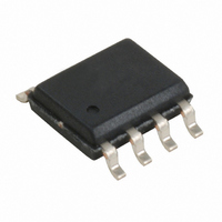
IC CLOCK GEN MPEG W/VCXO 8SOIC
Manufacturer
Cypress Semiconductor Corp
Type
Clock Generator, Fanout Distributionr
Datasheet
1.CY2412SXC-1.pdf
(5 pages)
Specifications of CY2412SXC-3T
Number Of Circuits
1
Package / Case
8-SOIC (3.9mm Width)
Pll
Yes
Input
Clock
Output
CMOS
Ratio - Input:output
1:3
Differential - Input:output
No/No
Frequency - Max
54MHz
Divider/multiplier
Yes/No
Voltage - Supply
3.14 V ~ 3.47 V
Operating Temperature
0°C ~ 70°C
Mounting Type
Surface Mount
Frequency-max
54MHz
Minimum Input Frequency
13.5 MHz
Output Frequency Range
13.5 MHz to 54 MHz
Supply Voltage (max)
3.47 V
Supply Voltage (min)
3.14 V
Maximum Operating Temperature
+ 70 C
Minimum Operating Temperature
0 C
Mounting Style
SMD/SMT
Operating Supply Voltage
3.3 V
Lead Free Status / RoHS Status
Lead free / RoHS Compliant


Pullable Crystal Specifications
Absolute Maximum Conditions
Recommended Operating Conditions
DC Electrical Characteristics
Document #: 38-07227 Rev. *F
Notes
F
C
R
R
DL
F
F
C
C
C
V
T
T
V
T
C
f
t
I
I
C
I
REF
PU
OH
OL
IZ
1. Crystals that meet this specification includes: Ecliptek ECX-5788-13.500M,Siward XTL001050A-13.5-14-400, Raltron A-13.500-14-CL,PDI HA13500XFSA14XC.
2. Float X
3. Rated for ten years.
A
NOM
3SEPHI
3SEPLO
DD
S
J
DD
LNOM
1
3
0
0/
1
LOAD
Parameter
IN
/R
C
Parameter
Parameter
Parameter
1
1
OUT
if X
IN
Output High Current
Output Low Current
Input Capacitance
Input Leakage Current
is externally driven.
Nominal crystal frequency
Nominal load capacitance
Equivalent series resistance (ESR)
Ratio of third overtone mode ESR to funda-
mental mode ESR
Crystal drive level
Third overtone separation from 3*F
Third overtone separation from 3*F
Crystal shunt capacitance
Ratio of shunt to motional capacitance
Crystal motional capacitance
Supply Voltage
Storage Temperature
Junction Temperature
Digital Inputs
Digital Outputs referred to V
Electrostatic Discharge
Operating Voltage
Ambient Temperature
Max. Load Capacitance
Reference Frequency
Power up time for all VDDs to reach minimum specified voltage (power ramps
must be monotonic)
Description
Description
[3]
[1]
V
V
OH
OL
DD
= 0.5, V
= V
Description
Description
NOM
NOM
DD
– 0.5, V
DD
= 3.3V
Test Conditions
Parallel resonance, fundamental
mode, AT cut
Fundamental mode
Ratio used because typical R
values are much less than the
maximum spec.
No external series resistor as-
sumed
High side
Low side
DD
= 3.3V
Condition
1
V
V
14.4
3.14
0.05
Min
Min
300
180
Min
SS
SS
12
12
–
–
–
3
–
–
–
0
–0.5
Min
–65
–
2
– 0.3
– 0.3
Typ.
Typ.
13.5
Typ.
13.5
3.3
0.5
18
24
14
24
–
–
–
–
–
–
5
V
V
DD
DD
Max
125
125
7.0
+ 0.3
+ 0.3
–150
Max
21.6
Max
3.47
Max
250
500
2.0
25
70
15
CY2412
–
–
–
–
7
7
Page 2 of 5
MHz
Unit
ppm
ppm
Unit
mW
Unit
MHz
Unit
pF
pF
pF
mA
mA
°C
°C
kV
ms
°C
pF
pF
μA
Ω
V
V
V
V
[+] Feedback
Related parts for CY2412SXC-3T
Image
Part Number
Description
Manufacturer
Datasheet
Request
R

Part Number:
Description:
Manufacturer:
Cypress Semiconductor Corp
Datasheet:
Part Number:
Description:
Manufacturer:
Cypress Semiconductor Corp
Datasheet:
Part Number:
Description:
Manufacturer:
Cypress Semiconductor Corp
Datasheet:
Part Number:
Description:
Manufacturer:
Cypress Semiconductor Corp
Datasheet:
Part Number:
Description:
Manufacturer:
Cypress Semiconductor Corp
Datasheet: