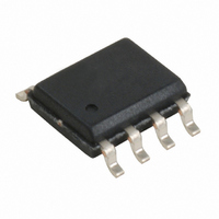
CY2412SXC-3T Cypress Semiconductor Corp, CY2412SXC-3T Datasheet - Page 3

CY2412SXC-3T
Manufacturer Part Number
CY2412SXC-3T
Description
IC CLOCK GEN MPEG W/VCXO 8SOIC
Manufacturer
Cypress Semiconductor Corp
Type
Clock Generator, Fanout Distributionr
Datasheet
1.CY2412SXC-1.pdf
(5 pages)
Specifications of CY2412SXC-3T
Number Of Circuits
1
Package / Case
8-SOIC (3.9mm Width)
Pll
Yes
Input
Clock
Output
CMOS
Ratio - Input:output
1:3
Differential - Input:output
No/No
Frequency - Max
54MHz
Divider/multiplier
Yes/No
Voltage - Supply
3.14 V ~ 3.47 V
Operating Temperature
0°C ~ 70°C
Mounting Type
Surface Mount
Frequency-max
54MHz
Minimum Input Frequency
13.5 MHz
Output Frequency Range
13.5 MHz to 54 MHz
Supply Voltage (max)
3.47 V
Supply Voltage (min)
3.14 V
Maximum Operating Temperature
+ 70 C
Minimum Operating Temperature
0 C
Mounting Style
SMD/SMT
Operating Supply Voltage
3.3 V
Lead Free Status / RoHS Status
Lead free / RoHS Compliant
DC Electrical Characteristics
AC Electrical Characteristics
Notes
Document #: 38-07227 Rev. *F
f
V
f
I
4. Not 100% tested.
ΔXO
VBW
DD
Parameter
VCXO
Parameter
DC
ER
EF
t
t
10
9
[4]
VCXO pullability range
VCXO input range
VCXO input bandwidth
Supply Current
Output Duty Cycle
Rising Edge Rate
Falling Edge Rate
Clock Jitter
PLL Lock Time
Figure 3. Rise and Fall Time Definitions: ER = 0.6 x VDD / t3 , EF = 0.6 x VDD / t4
Description
Description
V
DD
0.1 μF
CLK
(continued)
CLK
Figure 2. Duty Cycle Definition; DC = t2/t1
Duty Cycle is defined in
Clock Edge Rate, Measured from 20% to 80% of V
C
Output Clock Edge Rate, Measured from 80% to 20%
of V
Peak to Peak period jitter
LOAD
Sum of Core and Output Current
DD,
= 15 pF. See
C
LOAD
Figure 4. Test Circuit
OUTPUTS
50%
t1
t2
t3
= 15 pF. See
GND
20%
Test Conditions
80%
Test Conditions
Figure
Figure
50%
3.
Figure
t4
2, 50% of V
3.
DD
C
DD,
LOAD
CLK out
+150
Min
Min
0.8
0.8
45
0
DC to
Typ.
Typ.
200
100
1.4
1.4
50
Max
V
Max
200
35
55
CY2412
DD
3
Page 3 of 5
Unit
ppm
kHz
V/ns
V/ns
Unit
mA
ms
ps
V
%
[+] Feedback


