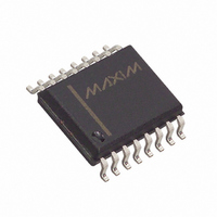
DS1021S-50+T&R Maxim Integrated Products, DS1021S-50+T&R Datasheet - Page 2

DS1021S-50+T&R
Manufacturer Part Number
DS1021S-50+T&R
Description
DELAY PROG 8-BIT .5NS 16-SOIC
Manufacturer
Maxim Integrated Products
Datasheet
1.DS1021S-25.pdf
(9 pages)
Specifications of DS1021S-50+T&R
Number Of Taps/steps
256
Function
Programmable
Delay To 1st Tap
10nS
Tap Increment
0.5nS
Available Total Delays
137.5ns
Voltage - Supply
4.75 V ~ 5.25 V
Operating Temperature
0°C ~ 70°C
Mounting Type
Surface Mount
Package / Case
16-SOIC (0.300", 7.5mm Width)
Lead Free Status / RoHS Status
Lead free / RoHS Compliant
Number Of Independent Delays
-
PARALLEL MODE (S = 1)
In the PARALLEL programming mode, the output of the DS1021 will reproduce the logic state of the
input after a delay determined by the state of the 8 program input pins P0 - P7. The parallel inputs can be
programmed using DC levels or computer-generated data. For infrequent modification of the delay value,
jumpers may be used to connect the input pins to V
timing adjustment, DIP switches should be used. The enable pin (E) must be at a logic 1 in hardwired
implementations.
Maximum flexibility is obtained when the 8 parallel programming bits are set using computer-generated
data. When the data setup (t
used to latch data supplied on an 8-bit bus. Enable must be held at a logic 1 if it is not used to latch the
data. After each change in delay value, a settling time (t
are accurately delayed.
Since the DS1021 is a CMOS design, unused input pins (D and C) must be connected to well-defined
logic levels; they must not be allowed to float.
SERIAL MODE (S = 0)
In the SERIAL programming mode, the output of the DS1021 will reproduce the logic state of the input
after a delay time determined by an 8-bit value clocked into serial port D. While observing data setup
(t
the serial clock (C). The enable pin (E) must be at a logic 1 to load or read the internal 8-bit input register,
during which time the delay is determined by the last value activated. Data transfer ends and the new
delay value is activated when enable (E) returns to a logic 0. After each change, a settling time (t
required before the delay is accurate.
As timing values are shifted into the serial data input (D), the previous contents of the 8-bit input register
are shifted out of the serial output pin (Q) in MSB-to-LSB order. By connecting the serial output of one
DS1021 to the serial input of a second DS1021, multiple devices can be daisy-chained (cascaded) for
programming purposes (Figure 3). The total number of serial bits must be eight times the number of units
daisy-chained and each group of 8 bits must be sent in MSB-to-LSB order.
Applications can read the setting of the DS1021 delay line by connecting the serial output pin (Q) to the
serial input (D) through a resistor with a value of 1K to 10K ohms (Figure 2). Since the read process is
destructive, the resistor restores the value read and provides isolation when writing to the device. The
resistor must connect the serial output (Q) of the last device to the serial input (D) of the first device of a
daisy-chain (Figure 3). For serial readout with automatic restoration through a resistor, the device used to
write serial data must go to a high impedance state.
To initiate a serial read, enable (E) is taken to a logic 1 while serial clock (C) is at a logic 0. After a
waiting time (t
the serial clock (C), bit 7 (MSB) is rewritten and bit 6 appears on the output after a time t
the input register to its original state, this clocking process must be repeated eight times. In the case of a
daisy-chain, the process must be repeated eight times per package. If the value read is restored before
enable (E) is returned to logic 0, no settling time (t
unchanged.
Since the DS1021 is a CMOS design, unused input pins (P1 - P7) must be connected to well-defined logic
levels; they must not be allowed to float. Serial output Q/P0 should be allowed to float if unused.
DSC
) and data hold (t
EQV
), bit 7 (MSB) appears on the serial output (Q). On the first rising (0 → 1) transition of
DHC
) requirements, timing data is loaded in MSB-to-LSB order by the rising edge of
DSE
) and data hold (t
2 of 9
DHE
EDV
) requirements are observed, the enable pin can be
CC
) is required and the programmed delay remains
and ground. For applications requiring frequent
EDV
or t
PDV
) is required before input logic levels
CQV
. To restore
EDV
) is


