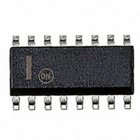
MC14536BDWG ON Semiconductor, MC14536BDWG Datasheet - Page 8

MC14536BDWG
Manufacturer Part Number
MC14536BDWG
Description
IC TIMER PROGR 24STAGE 16-SOIC
Manufacturer
ON Semiconductor
Type
Programmable Timerr
Specifications of MC14536BDWG
Frequency
2MHz
Voltage - Supply
3 V ~ 18 V
Current - Supply
15µA
Operating Temperature
-55°C ~ 125°C
Package / Case
16-SOIC (0.300", 7.5mm Width)
Number Of Internal Timers
1
Supply Voltage (max)
18 V
Supply Voltage (min)
3 V
Maximum Power Dissipation
500 mW
Maximum Operating Temperature
+ 125 C
Minimum Operating Temperature
- 55 C
Mounting Style
SMD/SMT
Propagation Delay (max)
3600 ns @ 5 V or 1300 ns @ 10 V or 1000 ns @ 15 V
Circuit Type
Low-Power Schottky
Current, Supply
600 μA
Function Type
24-Stages
Logic Function
Programmable
Logic Type
CMOS
Package Type
SOIC-16
Special Features
Binary
Temperature, Operating, Range
-55 to +125 °C
Voltage, Supply
3 to 18 VDC
Lead Free Status / RoHS Status
Lead free / RoHS Compliant
Count
-
Lead Free Status / Rohs Status
Lead free / RoHS Compliant
Other names
MC14536BDWG
MC14536BDWGOS
MC14536BDWGOS
Available stocks
Company
Part Number
Manufacturer
Quantity
Price
Company:
Part Number:
MC14536BDWG
Manufacturer:
ON
Quantity:
2 416
reduction of test time required to exercise all 24 counter
stages. This test function divides the counter into three
8−stage sections and 255 counts are loaded in each of the
8−stage sections in parallel. All flip−flops are now at a “1”.
The counter is now returned to the normal 24−stages in
series configuration. One more pulse is entered into In
which will cause the counter to ripple from an all “1” state
to an all “0” state.
GENERATOR
Test function (Figure 10) has been included for the
PULSE
FUNCTIONAL TEST SEQUENCE
Figure 8. Power Dissipation Test
In
1
1
0
1
0
−
−
−
0
0
1
0
20 ns
1
FUNCTIONAL TEST SEQUENCE
Circuit and Waveform
500 mF
Set
10%
0
1
1
1
1
0
0
0
DUTY CYCLE
90%
Inputs
SET
RESET
8−BYPASS
IN
C INH
MONO−IN
OSC INH
A
B
C
D
50%
1
Reset
50%
DECODE
1
1
1
1
1
0
0
0
I
D
OUT 1
V
OUT
OUT
V
DD
SS
2
8−Bypass
0.01 mF
CERAMIC
20 ns
1
1
1
1
1
0
0
0
C
C
C
L
L
L
Q1 thru Q24
Decade Out
Outputs
GENERATOR
PULSE
0
0
0
1
1
1
0
http://onsemi.com
MC14536B
1
Counter is in three 8 stage sections in parallel mode.
First “1” to “0” transition of clock.
255 “1” to “0” transitions are clocked in the counter.
The 255 “1” to “0” transition.
Counter converted back to 24 stages in series mode.
Set and Reset must be connected together and simultaneously
go from “1” to “0”.
In
Counter Ripples from an all “1” state to an all “0” state.
1
8
Figure 9. Switching Time Test Circuit and Waveforms
Switches to a “1”.
Figure 10. Functional
SET
RESET
8−BYPASS
IN
C INH
MONO−IN
OSC INH
A
B
C
D
1
Test Circuit
All 24 stages are in Reset mode.
DECODE
OUT 1
V
V
OUT
OUT
DD
SS
2
Comments
20 ns
OUT
IN
GENERATOR
t
1
PLH
C
PULSE
L
t
WL
10%
90%
t
TLH
SET
RESET
8−BYPASS
IN
C INH
MONO−IN
OSC INH
A
B
C
D
1
20 ns
50%
DECODE
t
THL
OUT 1
V
V
OUT
OUT
DD
SS
t
WH
2
50%
t
PHL


