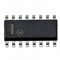
MC14536BDWG ON Semiconductor, MC14536BDWG Datasheet - Page 9

MC14536BDWG
Manufacturer Part Number
MC14536BDWG
Description
IC TIMER PROGR 24STAGE 16-SOIC
Manufacturer
ON Semiconductor
Type
Programmable Timerr
Specifications of MC14536BDWG
Frequency
2MHz
Voltage - Supply
3 V ~ 18 V
Current - Supply
15µA
Operating Temperature
-55°C ~ 125°C
Package / Case
16-SOIC (0.300", 7.5mm Width)
Number Of Internal Timers
1
Supply Voltage (max)
18 V
Supply Voltage (min)
3 V
Maximum Power Dissipation
500 mW
Maximum Operating Temperature
+ 125 C
Minimum Operating Temperature
- 55 C
Mounting Style
SMD/SMT
Propagation Delay (max)
3600 ns @ 5 V or 1300 ns @ 10 V or 1000 ns @ 15 V
Circuit Type
Low-Power Schottky
Current, Supply
600 μA
Function Type
24-Stages
Logic Function
Programmable
Logic Type
CMOS
Package Type
SOIC-16
Special Features
Binary
Temperature, Operating, Range
-55 to +125 °C
Voltage, Supply
3 to 18 VDC
Lead Free Status / RoHS Status
Lead free / RoHS Compliant
Count
-
Lead Free Status / Rohs Status
Lead free / RoHS Compliant
Other names
MC14536BDWG
MC14536BDWGOS
MC14536BDWGOS
Available stocks
Company
Part Number
Manufacturer
Quantity
Price
Company:
Part Number:
MC14536BDWG
Manufacturer:
ON
Quantity:
2 416
NOTE: When power is first applied to the device, DECODE OUT can be either at a high or low state. On the rising edge of a SET pulse
Figure 11. Time Interval Configuration Using an External Clock, Set, and Clock Inhibit Functions
the output goes high if initially at a low state. The output remains high if initially at a high state. Because CLOCK INH is held
high, the clock source on the input pin has no effect on the output. Once CLOCK INH is taken low, the output goes low on the
first negative clock transition. The output returns high depending on the 8−BYPASS, A, B, C, and D inputs, and the clock input
period. A 2
A 2
0
–divided output of IN
PULSE
GEN.
n
frequency division (where n = the number of stages selected from the truth table) is obtainable at DECODE OUT.
PULSE
GEN.
DECODE OUT
CLOCK INH
1
can be obtained at OUT
SET
IN
CLOCK
1
POWERUP
(Divide−by−2 Configured)
http://onsemi.com
MC14536B
1
and OUT
10
11
12
14
15
6
9
2
1
7
3
9
8−BYPASS
A
B
C
D
RESET
OSC INH
MONO−IN
SET
CLOCK INH
IN
2
1
.
V
V
+V
DD
SS
16
8
DECODE OUT
OUT 1
OUT 2
13
4
5


