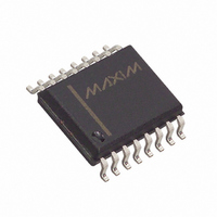
DS4026S+HCN Maxim Integrated Products, DS4026S+HCN Datasheet - Page 12

DS4026S+HCN
Manufacturer Part Number
DS4026S+HCN
Description
IC TCXO 19.44MHZ 16-SOIC
Manufacturer
Maxim Integrated Products
Type
Temperature, Compensated Crystal Oscillator (TCXO)r
Datasheet
1.DS4026SYCN.pdf
(14 pages)
Specifications of DS4026S+HCN
Frequency
19.44MHz
Voltage - Supply
3.135 V ~ 3.465 V
Current - Supply
1.5mA
Operating Temperature
-40°C ~ 85°C
Package / Case
16-SOIC (0.300", 7.5mm Width)
Lead Free Status / RoHS Status
Lead free / RoHS Compliant
Count
-
10MHz to 51.84MHz TCXO
The DS4026 can operate in the following two modes:
12
Slave receiver mode (write mode): Serial data and
clock are received through SDA and SCL. After each
byte is received, an acknowledge bit is transmitted.
START and STOP conditions are recognized as the
beginning and end of a serial transfer. Address
recognition is performed by hardware after reception
of the slave address and direction bit. The slave
address byte is the first byte received after the mas-
ter generates a START condition. The slave address
byte contains the 7-bit DS4026 address, which is
1000001, followed by the direction bit (R/W), which is
0 for a write. After receiving and decoding the slave
address byte, the DS4026 outputs an acknowledge
on SDA. After the DS4026 acknowledges the slave
address and write bit, the master transmits a word
address to the DS4026. This sets the register pointer
on the DS4026, with the DS4026 acknowledging the
transfer. The master can then transmit zero or more
bytes of data, with the DS4026 acknowledging each
byte received. The register pointer increments after
each data byte is transferred. The master generates
a STOP condition to terminate the data write.
______________________________________________________________________________________
Slave transmitter mode (read mode): The first byte
is received and handled as in the slave receiver
mode. However, in this mode, the direction bit indi-
cates that the transfer direction is reversed. Serial
data is transmitted on SDA by the DS4026 while the
serial clock is input on SCL. START and STOP condi-
tions are recognized as the beginning and end of a
serial transfer. Address recognition is performed by
hardware after reception of the slave address and
direction bit. The slave address byte is the first byte
received after the master generates a START condi-
tion. The slave address byte contains the 7-bit
DS4026 address, which is 1000001, followed by the
direction bit (R/W), which is 1 for a read. After receiv-
ing and decoding the slave address byte, the
DS4026 outputs an acknowledge on SDA. The
DS4026 then begins to transmit data starting with the
register address pointed to by the register pointer. If
the register pointer is not written to before the initia-
tion of a read mode, the first address that is read is
the last one stored in the register pointer. The
DS4026 must receive a not acknowledge to end a
read.


