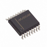
DS4026S+HCN Maxim Integrated Products, DS4026S+HCN Datasheet - Page 9

DS4026S+HCN
Manufacturer Part Number
DS4026S+HCN
Description
IC TCXO 19.44MHZ 16-SOIC
Manufacturer
Maxim Integrated Products
Type
Temperature, Compensated Crystal Oscillator (TCXO)r
Datasheet
1.DS4026SYCN.pdf
(14 pages)
Specifications of DS4026S+HCN
Frequency
19.44MHz
Voltage - Supply
3.135 V ~ 3.465 V
Current - Supply
1.5mA
Operating Temperature
-40°C ~ 85°C
Package / Case
16-SOIC (0.300", 7.5mm Width)
Lead Free Status / RoHS Status
Lead free / RoHS Compliant
Count
-
The output driver is a CMOS square-wave output with
symmetrical rise and fall time.
The temperature sensor provides a 12-bit temperature
reading with a resolution of 0.0625°C. The sensor is in
continuous conversion mode. If DCOMP is set, conver-
sions continue but temperature updates are inhibited.
The controller coordinates the conversion of tempera-
ture into digital codes. When the temperature reading is
different from the previous one or the frequency tuning
register is changed, the controller looks up the two cor-
responding capacitance trim codes from the lookup
table at a 0.5°C increment. The trim codes are interpo-
lated to 0.0625°C resolution.
The result is added with the tuning value from the fre-
quency tuning register and loaded into the DAC regis-
ters to adjust voltage output. The monotonic DAC
provides an analog voltage based on temperature
compensation to drive the variable capacitor.
The DS4026 operates as a slave device on the serial
bus. Access is obtained by implementing a START
condition and providing a device identification code fol-
lowed by data. Subsequent registers can be accessed
sequentially until a STOP condition is executed.
ADDRESS
ADDRESS
POR
POR
POR
POR
00h
01h
02h
03h
DCOMP
BIT 7
BIT 7
Data
Data
Sign
_______________________________________________________________________________________
0
0
0
0
BIT 6
BIT 6
Data
Sign
Data
Data
0
0
0
0
BIT 5
BIT 5
Data
Data
Data
Data
0
0
0
0
10MHz to 51.84MHz TCXO
Frequency Tuning Register (00h–01h), POR = 00h
BIT 4
BIT 4
Data
Data
Data
Data
0
0
0
0
DCOMP is bit 7 of the frequency tuning register (see
the Frequency Tuning Register (00h–01h), POR = 00h
table). When set to logic 1, this bit’s temperature-com-
pensation function is disabled. This disabling prevents
the variable capacitor in the oscillator block from
changing. However, the temperature register still per-
forms temperature conversions. The temperature trim
code from the last temperature conversion before
DCOMP is enabled is used for temperature compensa-
tion. The FTUNE registers are still functional when
DCOMP is disabled.
The frequency tuning registers adjust the base frequen-
cy. The frequency tuning value is represented in two’s
complement data. Bit 6 of FTUNEH is the sign, bit 5 is
the MSB, and bit 0 of FTUNEL is the LSB (see Table 1).
When the tuning register low (01h) is programmed with
a value, the next temperature update cycle sums the
programmed value with the factory compensated
value. This allows the user to digitally control the base
frequency using the I
These frequency tuning register bits allow the tuning of
the base frequency. Each bit typically represents
about 1ppb (typ). For FTUNEH = 3Fh and FTUNEL =
FFh, the device pushes the base frequency by approx-
imately +15ppm.
Disable Compensation Update (DCOMP)
BIT 3
BIT 3
Data
Data
Data
0
0
0
0
0
Temperature Register (02h–03h)
BIT 2
2
BIT 2
Data
Data
Data
C protocol.
0
0
0
0
0
BIT 1
BIT 1
Data
Data
Address Map
Data
0
0
0
0
0
BIT 0
BIT 0
Data
Data
Data
0
0
0
0
0
9


