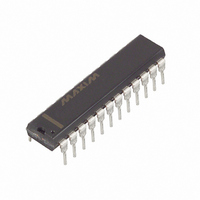
DS17887-5+ Maxim Integrated Products, DS17887-5+ Datasheet - Page 14

DS17887-5+
Manufacturer Part Number
DS17887-5+
Description
IC RTC 5V 8K NV RAM 24-EDIP
Manufacturer
Maxim Integrated Products
Type
Clock/Calendar/NVSRAMr
Datasheet
1.DS17285S-5.pdf
(31 pages)
Specifications of DS17887-5+
Memory Size
64K (8K x 8)
Time Format
HH:MM:SS (12/24 hr)
Date Format
YY-MM-DD-dd
Interface
Parallel
Voltage - Supply
4.5 V ~ 5.5 V
Operating Temperature
0°C ~ 70°C
Mounting Type
Through Hole
Package / Case
24-DIP (600 mil) Module
Function
Clock/Calendar/Alarm
Rtc Memory Size
8192 Byte
Supply Voltage (max)
5.5 V
Supply Voltage (min)
4.5 V
Maximum Operating Temperature
+ 70 C
Minimum Operating Temperature
0 C
Mounting Style
Through Hole
Rtc Bus Interface
Multiplexed
Supply Current
25 mA
Lead Free Status / RoHS Status
Lead free / RoHS Compliant
The four control registers (A, B, C, and D) reside in
Real-Time Clocks
Bit 7: Update In Progress (UIP). This bit is a status
flag that can be monitored. When the UIP bit is 1, the
update transfer will soon occur. When UIP is 0, the
update transfer does not occur for at least 244µs. The
time, calendar, and alarm information in RAM is fully
available for access when the UIP bit is 0. The UIP bit is
read-only. Writing the SET bit in Register B to 1 inhibits
any update transfer and clears the UIP status bit.
Table 3B. Time, Calendar, and Alarm Data Modes—Binary Mode (DM = 1)
Note: Unless otherwise specified, the state of the registers is not defined when power is first applied. Except for the seconds regis-
ter, 0 bits in the time and date registers can be written to 1, but can be modified when the clock updates. 0 bits should always be
written to 0 except for alarm mask bits.
Register A (0Ah)
MSB
14
Bank 1, 48h
Bank 1, 49h
ADDRESS
0Ch
0Dh
BIT 7
0Ah
0Bh
00h
01h
02h
03h
04h
05h
06h
07h
08h
09h
UIP
____________________________________________________________________
AM/PM
AM/PM
BIT 7
IRQF
SET
VRT
UIP
0
0
0
0
0
0
0
0
0
0
BIT 6
DV2
BIT 6
DV2
10 Century
PIE
PF
Control Registers
0
0
0
0
0
0
0
0
0
0
10 Date
BIT 5
DV1
BIT 5
DV1
AIE
AF
0
0
0
0
0
0
BIT 4
DV0
UIE
UF
0
0
0
0
0
BIT 4
DV0
SQWE
BIT 3
Year
RS3
0
0
0
Seconds
Seconds
Minutes
Minutes
Hours
Hours
BIT 2
Date
RS2
DM
both bank 0 and bank 1. These registers are accessi-
ble at all times, even during the update cycle.
Bits 6, 5, and 4: DV2, DV1, and DV0. These bits are
used to turn the oscillator on or off and to reset the
countdown chain. A pattern of 01X is the only combina-
tion of bits that turns the oscillator on and allows the RTC
to keep time. A pattern of 11X enables the oscillator but
holds the countdown chain in reset. The next update
occurs at 500ms after a pattern of 01X is written to DV0,
DV1, and DV2. DV0 is used to select bank 0 or bank 1 as
defined in Table 5. When DV0 is set to 0, bank 0 is
selected. When DV0 is set to 1, bank 1 is selected.
0
0
Century
BIT 3
Month
Hours
Hours
RS3
Date
24/12
BIT 1
Day
RS1
0
0
BIT 0
DSE
RS0
0
0
BIT 2
RS2
Seconds Alarm
Minutes Alarm
Hours Alarm
FUNCTION
Date Alarm
Seconds
Minutes
Century
Control
Control
Control
Control
Hours
Month
Date
Year
Day
BIT 1
RS1
1–0C +AM/PM
1–0C +AM/PM
RANGE
01–0C
00–3B
00–3B
00–3B
00–3B
00–17
00–17
01–07
01–1F
00–63
00–63
01–1F
—
—
—
—
BIT 0
RS0
LSB


