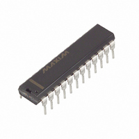
DS17887-5+ Maxim Integrated Products, DS17887-5+ Datasheet - Page 23

DS17887-5+
Manufacturer Part Number
DS17887-5+
Description
IC RTC 5V 8K NV RAM 24-EDIP
Manufacturer
Maxim Integrated Products
Type
Clock/Calendar/NVSRAMr
Datasheet
1.DS17285S-5.pdf
(31 pages)
Specifications of DS17887-5+
Memory Size
64K (8K x 8)
Time Format
HH:MM:SS (12/24 hr)
Date Format
YY-MM-DD-dd
Interface
Parallel
Voltage - Supply
4.5 V ~ 5.5 V
Operating Temperature
0°C ~ 70°C
Mounting Type
Through Hole
Package / Case
24-DIP (600 mil) Module
Function
Clock/Calendar/Alarm
Rtc Memory Size
8192 Byte
Supply Voltage (max)
5.5 V
Supply Voltage (min)
4.5 V
Maximum Operating Temperature
+ 70 C
Minimum Operating Temperature
0 C
Mounting Style
Through Hole
Rtc Bus Interface
Multiplexed
Supply Current
25 mA
Lead Free Status / RoHS Status
Lead free / RoHS Compliant
The timing associated with both the wake-up and kick-
starting sequences is illustrated in the Wake-
Up/Kickstart Timing Diagram (Figure 6). The timing
associated with these functions is divided into five inter-
vals, labeled 1 to 5 on the diagram.
The occurrence of either a kickstart or wake-up condition
causes the PWR pin to be driven low, as described
above. During interval 1, if the supply voltage on the
DS17x85/DS17x87 V
V
expires, then PWR remains at the active-low level. If V
does not rise above the greater of V
time, then the PWR output pin is turned off and returns to
its high-impedance level. In this event, the IRQ pin also
Figure 6. Wake-Up/Kickstart Timing Diagram
Table 6. Wake-Up/Kickstart Timing
(T
Note: Wake-up/kickstart timeout is generated only when the oscillator is enabled and the countdown chain is not reset.
Kickstart-Input Pulse Width
Wake-Up/Kickstart Power-On
Timeout
BAT
A
=+25°C)
or V
*CONDITION
VPF < VBAT
*CONDITION
VBAT > VPF
WF/KF
(INTERNAL)
KS
PWR
IRQ
*THIS CONDITION CAN OCCUR WITH THE 3V DEVICE.
NOTE: THE TIME INTERVALS SHOWN ABOVE ARE REFERENCED IN THE WAKE-UP/KICKSTART SECTION.
PARAMETER
PF
HIGH-IMPEDANCE
HIGH-IMPEDANCE
before the power-on timeout period (t
V
V
0V
V
V
0V
V
V
V
V
V
V
BAT
PF
PF
BAT
IH
IH
IL
IH
IL
IL
CC
pin rises above the greater of
t
KSPW
t
POTP
SYMBOL
t
t
KSPW
POTO
1
BAT
____________________________________________________________________
or V
2
PF
in this
POTO
CC
)
CONDITIONS
remains tri-stated. The interrupt flag bit (either WF or KF)
associated with the attempted power-on sequence
remains set until cleared by software during a subse-
quent system power-on.
If V
tem power-on sequence continue as shown in intervals
2 to 5 in the timing diagram. During interval 2, PWR
remains active and IRQ is driven to its active-low level,
indicating that either WF or KF was set in initiating the
power-on. In the diagram KS is assumed to be pulled
up to the V
automatically cleared to 0 in response to a successful
power-on. The PWR line remains active as long as the
PAB remains cleared to 0.
CC
3
is applied within the timeout period, then the sys-
BAUX
Real-Time Clocks
supply. Also at this time, the PAB bit is
MIN
2
2
4
TYP
5
MAX
UNITS
µs
s
23


