DS1643P-100+ Maxim Integrated Products, DS1643P-100+ Datasheet
DS1643P-100+
Specifications of DS1643P-100+


Related parts for DS1643P-100+


DS1643P-100+ Summary of contents
Page 1
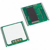
... DS164XP Timekeeping RAM ORDERING INFORMATION VOLTAGE RANGE PART DS1643-85+ DS1643-100+ DS1643P-85+ DS1643P-100+ * DS9034I-PCX+ and DS9034-PCX+ required (must be ordered separately). +Denotes a lead(Pb)-free/RoHS-compliant package. The top mark will include a “+” symbol on lead-free devices. Nonvolatile Timekeeping RAMs PIN CONFIGURATIONS TOP VIEW TEMP RANGE (V) 5 ...
Page 2
... V No Connection Address Inputs Data Input/Output Active-Low Chip-Enable Input Active-Low Output-Enable Input Chip-Enable 2 Input (Active High) Active-Low Write-Enable Input Power-Supply Input CC Active-Low Power-Fail Output. This open-drain pin requires a pullup resistor for proper operation. Ground Crystal Connection, Battery Connection BAT DS1643/DS1643P FUNCTION ...
Page 3
... This design allows the PowerCap to be mounted on top of the DS1643P after the completion of the surface mount process. Mounting the PowerCap after the surface mount process prevents damage to the crystal and battery due to high temperatures required for solder reflow ...
Page 4
... X X Deselect X X Deselect X V Write Read Read Deselect X X Deselect bit is the MSB for the seconds registers. Setting it to OSC DS1643/DS1643P DQ POWER High Z Standby High Z Standby Data In Active Data Out Active High-Z Active High-Z CMOS Standby High-Z Data Retention Mode ...
Page 5
... The DS1643 is guaranteed to keep time accuracy to within 1 minute per month at 25C. CLOCK ACCURACY (POWERCAP MODULE) The DS1643P and DS9034PCX are each individually tested for accuracy. Once mounted together, the module is guaranteed to keep time accuracy to within 1.53 minutes per month (35ppm) at 25C. ...
Page 6
... At this time the power-on reset output signal ( CE returns to nominal levels. When powered down. CC supply is not present. The capability of this internal power supply DS1643/DS1643P (point at which write PF RST falls below the CC pin to the internal battery and CC is returned to nominal CC , all control, data, ...
Page 7
... Output Leakage Current (Any Output) Output Logic 1 Voltage (I = -1.0mA) OUT Output Logic 0 Voltage (I = +2.1mA) OUT Write Protection Voltage SYMBOL MIN TYP V 4 -0.3 IL SYMBOL MIN TYP CC1 I 1 CC2 2 4.25 4. DS1643/DS1643P MAX UNITS NOTES 5 0 +0.8 V MAX UNITS NOTES A +1 0 ...
Page 8
... Access Time OE Data Off Time OE Output Hold from Address READ CYCLE TIMING DIAGRAM 85ns SYMBOL ACCESS MIN MAX CEL t 85 CEA t 95 CE2A t 30 CEZ t 5 OEL t 45 OEA t 30 OEZ DS1643/DS1643P 100ns ACCESS UNITS NOTES MIN MAX 100 ns 100 100 ns 105 ...
Page 9
... Pulse Width WE Pulse Width CE CE2 Pulse Width Data Setup Time Data Hold Time Address Hold Time Data Off Time WE Write Recovery Time 85ns SYMBOL ACCESS MIN MAX WEW t 70 CEW t 75 CE2W WEZ DS1643/DS1643P 100ns ACCESS UNITS NOTES MIN MAX 100 ...
Page 10
... WRITE CYCLE TIMING DIAGRAM—WE CONTROLLED WRITE CYCLE TIMING DIAGRAM— , CE2 CONTROLLED DS1643/DS1643P ...
Page 11
... Power-Up Recover Time Expected Data Retention Time (Oscillator On) POWER-UP/POWER-DOWN TIMING CAPACITANCE (T = +25C) A PARAMETER Capacitance on All Pins Capacitance on All Output Pins SYMBOL MIN TYP 300 REC SYMBOL MIN TYP DS1643/DS1643P MAX UNITS NOTES s s s years 5, 6 MAX UNITS NOTES ...
Page 12
... RoHS status only. Package drawings may show a different suffix character, but the drawing pertains to the package regardless of RoHS status. PACKAGE TYPE 28 EDIP 34 PowerCap signal except that the logic levels for CE PACKAGE CODE MDF28+2 PC1 DS1643/DS1643P is first applied by the CC starting CC DOCUMENT NO. 21-0245 21-0246 ...
Page 13
... E IN. 0.015 MM 0.38 F IN. 0.140 MM 3.56 G IN. 0.090 MM 2.29 H IN. 0.590 MM 14.99 J IN. 0.010 MM 0.25 K IN. 0.015 MM 0. DS1643/DS1643P MAX 1.490 37.85 0.740 18.80 0.335 9.02 0.105 2.67 0.030 0.76 0.180 4.57 0.110 2.79 0.630 16.00 0.018 0.45 0.025 0.58 ...
Page 14
... SECONDS. TO SOLDER, APPLY FLUX TO THE PAD, HEAT THE LEAD FRAME PAD AND APPLY SOLDER. TO REMOVE THE PART, APPLY FLUX, HEAT THE LEAD FRAME PAD UNTIL THE SOLDER REFLOWS AND USE A SOLDER WICK TO REMOVE SOLDER DS1643/DS1643P MAX 0.930 0.990 - 0.080 0.058 0.052 ...
Page 15
... DS1643P WITH DS9034PCX ATTACHED PKG INCHES DIM MIN NOM A 0.920 0.925 B 0.955 0.960 C 0.240 0.245 D 0.052 0.055 E 0.048 0.050 F 0.015 0.020 G 0.020 0.025 DS1643/DS1643P MAX 0.930 0.965 0.250 0.058 0.052 0.025 0.030 ...
Page 16
... RECOMMENDED POWERCAP MODULE LAND PATTERN PKG INCHES DIM MIN NOM A - 1.050 B - 0.826 C - 0.050 D - 0.030 E - 0.112 DS1643/DS1643P MAX - - - - - ...
Page 17
... Maxim cannot assume responsibility for use of any circuitry other than circuitry entirely embodied in a Maxim product. No circuit patent licenses are implied. Maxim reserves the right to change the circuitry and specifications without notice at any time © 2010 Maxim Integrated Products DESCRIPTION Maxim is a registered trademark of Maxim Integrated Products, Inc. DS1643/DS1643P PAGES CHANGED ...