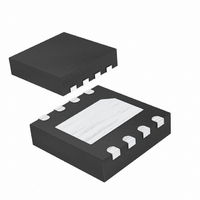
MAX6902ETA+T Maxim Integrated Products, MAX6902ETA+T Datasheet - Page 13

MAX6902ETA+T
Manufacturer Part Number
MAX6902ETA+T
Description
IC RTC SPI COMPAT 8-TDFN
Manufacturer
Maxim Integrated Products
Type
Clock/Calendar/NVSRAMr
Datasheet
1.MAX6902ETAT.pdf
(20 pages)
Specifications of MAX6902ETA+T
Memory Size
31B
Time Format
HH:MM:SS (12/24 hr)
Date Format
YY-MM-DD-dd
Interface
SPI, 3-Wire Serial
Voltage - Supply
2 V ~ 5.5 V
Operating Temperature
-40°C ~ 85°C
Mounting Type
Surface Mount
Package / Case
8-TDFN Exposed Pad
Lead Free Status / RoHS Status
Lead free / RoHS Compliant
Other names
MAX6902ETA+TTR
CS serves two functions. First, CS turns on the control
logic that allows access to the Shift register for
Address/Command and data transfer. Second, CS pro-
vides a method of terminating either single-byte or mul-
tiple-byte data transfers. All data transfers are initiated
by driving CS low. If CS is high, then DOUT is high
impedance.
A clock cycle on SCLK is a rising edge followed by a
falling edge. For data input, data must be valid at DIN
before the rising edge of the clock. For data outputs, bits
are valid on DOUT after the falling edge of the clock.
Following the eight SCLK cycles that input a Single-Byte
Write Address/Command, data bits are input on the ris-
ing edges of the next eight SCLK cycles. Additional
SCLK cycles are ignored. Input data MSB first.
Following the eight SCLK cycles that input a Burst-Write
Address/Command, data bits are input on the rising
edges of the following SCLK cycles. The number of
clock cycles depends on whether the timekeeping reg-
isters or RAM are being written. A Clock Burst Write
requires 1 Address/Command byte, 7 timekeeping data
bytes, and 1 Control register byte. A Burst Write to RAM
may be terminated after any complete data byte by dri-
ving CS high. Input data MSB first (Figure 3).
Figure 5. SPI Bus Timing Diagrams
CS
SCLK
DIN
DOUT
t
DS
t
CSS
D7
Data Input (Single-Byte Write)
______________________________________________________________________________________
t
DH
t
CL
Data Input (Burst Write)
D6
t
CH
D5
Serial Clock
Chip Select
SPI-Compatible RTC in a TDFN
D0
A read from the MAX6902 is initiated by an
Address/Command Write from the microcontroller (mas-
ter) to the MAX6902 (slave). The Address/Command
Write portion of the data transfer is clocked into the
MAX6902 on rising clock edges. Following the eighth
falling clock edge of SCLK, after t
begins to be output on DOUT of the MAX6902. Data
bytes are output MSB first. Additional SCLK cycles
transmit additional data bits, as long as CS remains low.
This permits continuous burst-mode read capability.
The MAX6902 is designed to use a standard
32.768kHz watch crystal. Table 1 details the recom-
mended crystal requirements. Some suggested crys-
tals are listed in Table 3. In addition to the specified
SMT devices, some of the listed manufacturers also
offer other package options.
Timekeeping accuracy of the MAX6902 is dependent
on the frequency stability, of the external crystal. To
determine frequency stability, use the parabolic curve
in Figure 6 and the following equations:
where:
Δf = change in frequency from +25°C (Hz)
f = nominal crystal frequency (Hz)
t
CP
t
DO
Frequency Stability and Temperature
D7
Applications Information
Data Output (Single-Byte Read
Δf fk
= (T - T)
0
2
Crystal Selection
and Burst Read)
DO
t
CSZ
(Figure 4) data
D0
t
CSH
t
CSW
13


