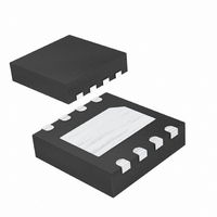
MAX6902ETA+T Maxim Integrated Products, MAX6902ETA+T Datasheet - Page 9

MAX6902ETA+T
Manufacturer Part Number
MAX6902ETA+T
Description
IC RTC SPI COMPAT 8-TDFN
Manufacturer
Maxim Integrated Products
Type
Clock/Calendar/NVSRAMr
Datasheet
1.MAX6902ETAT.pdf
(20 pages)
Specifications of MAX6902ETA+T
Memory Size
31B
Time Format
HH:MM:SS (12/24 hr)
Date Format
YY-MM-DD-dd
Interface
SPI, 3-Wire Serial
Voltage - Supply
2 V ~ 5.5 V
Operating Temperature
-40°C ~ 85°C
Mounting Type
Surface Mount
Package / Case
8-TDFN Exposed Pad
Lead Free Status / RoHS Status
Lead free / RoHS Compliant
Other names
MAX6902ETA+TTR
Each data transfer into or out of the MAX6902 is initiated
by an Address/Command byte. The Address/Command
byte specifies which registers are to be accessed, and
if the access is a read or a write. Figure 2 shows the
Address/Command bytes and their associated regis-
ters, and Table 2 lists the hex codes for all read and
write operations. The Address/Command bytes are
input MSB (bit 7) first. Bit 7 specifies a write (logic 0) or
read (logic 1). Bit 6 specifies register data (logic 0) or
RAM data (logic 1). Bits 5–1 specify the designated reg-
ister to be written or read. The LSB (bit 0) must be logic
1. If the LSB is a zero, writes to the MAX6902 are dis-
abled.
Sending the Clock Burst Address/Command (3Fh for
Write and BFh for Read), specifies burst-mode opera-
tion. In this mode, multiple bytes are read or written
after a single Address/Command. The first seven
clock/calendar registers (Seconds, Minutes, Hours,
Date, Month, Day, and Year) and the Control register
are consecutively read or written, starting with the MSB
of the Seconds register. When writing to the clock reg-
isters in burst mode, all seven clock/calendar registers
and the Control register must be written in order for the
data to be transferred. See Example: Setting the Clock
with a Burst Write.
Sending the RAM Burst Address/Command (F7h for
Write, FFh for Read) specifies burst-mode operation. In
this mode, the 31 RAM locations can be consecutively
read or written, starting at 41h for Writes, and C1h for
Reads. A Burst Read outputs all 31 bytes of RAM.
When writing to RAM in burst mode, it is not necessary
to write all 31 bytes for the data to transfer; each com-
plete byte written is transferred to RAM. When reading
from RAM, data are output until all 31 bytes have been
read, or until CS is driven high.
The time and date are set by writing to the timekeeping
registers (Seconds, Minutes, Hours, Date, Month, Day,
Year, and Century). During a write operation, an input
buffer accepts the new time data while the timekeeping
registers continue to increment normally, based on the
crystal counter. The buffer also keeps the timekeeping
registers from changing as the result of an incomplete
write operation, and collision-detection circuitry
ensures that a Time Write does not occur coincident
Writing to the Timekeeping Registers
_______________________________________________________________________________________
Command and Control
Address/Command Byte
Setting the Clock
Clock Burst Mode
RAM Burst Mode
SPI-Compatible RTC in a TDFN
with a Seconds register increment. The updated time
data are loaded into the timekeeping registers after the
rising edge of CS, at the end of the SPI write operation.
An incomplete write operation aborts the update proce-
dure, and the contents of the input buffer are discard-
ed. The timekeeping registers reflect the new time
beginning with the first Seconds register increment
after the rising edge of CS.
Although both Single Writes and Burst Writes are possi-
ble, the best way to write to the timekeeping registers is
with a Burst Write. With a Burst Write, the main time-
keeping registers (Seconds, Minutes, Hours, Date,
Month, Day, Year) and the Control register are written
sequentially following the Address/Command byte.
They must be written as a group of eight registers, with
8 bits each, for proper execution of the Burst Write
function. All seven timekeeping registers are simultane-
ously loaded into the clock counters by the rising edge
of CS, at the end of the SPI write operation. For a nor-
mal burst data transfer, the worst-case error that can
occur between the actual time and the written time
update is 1s.
If single write operations are used to enter data into the
timekeeping registers, error checking is required. If not
writing to the Seconds register, begin by reading the
Seconds register and save it as initial-seconds. Then
write to the required timekeeping registers, and finally
read the Seconds register again (final-seconds). Check
to see that final-seconds is equal to initial-seconds. If
not, repeat the write process. If writing to the Seconds
register, update the Seconds register first, and then
read it back and store its value (initial-seconds).
Update the remaining timekeeping registers and then
read the Seconds register again (final-seconds). Check
to see that final-seconds is equal to initial-seconds. If
not, repeat the write process.
Note: After writing to any time or date register, no read
or write operations are allowed for 45µs.
Bit 7 of the Hours register selects 12hr or 24hr mode.
When high, 12hr mode is selected. In 12hr mode, bit 5 is
the AM/PM bit, logic high for PM. In 24hr mode, bit 5 is
the second 10hr bit, logic high for hours 20 through 23.
Bit 7 of the Control register is the Write-Protect bit.
When high, the Write-Protect bit prevents write opera-
tions to all registers except itself. After initial settings
are written to the timekeeping registers, set the Write-
Protect bit to logic 1 to prevent erroneous data from
entering the registers during power glitches or inter-
rupted serial transfers. The lower 7 bits (bits 0–6) are
AM/PM and 12Hr/24Hr Mode
Write-Protect Bit
9


