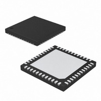
MAX19707ETM+ Maxim Integrated Products, MAX19707ETM+ Datasheet - Page 28

MAX19707ETM+
Manufacturer Part Number
MAX19707ETM+
Description
IC ANLG FRONT END 45MSPS 48-TQFN
Manufacturer
Maxim Integrated Products
Datasheet
1.MAX19707ETM.pdf
(37 pages)
Specifications of MAX19707ETM+
Number Of Bits
10
Number Of Channels
4
Power (watts)
84.6mW
Voltage - Supply, Analog
3V
Voltage - Supply, Digital
3V
Package / Case
48-TQFN Exposed Pad
Lead Free Status / RoHS Status
Lead free / RoHS Compliant
10-Bit, 45Msps, Ultra-Low-Power
Analog Front-End
The conversion requires 12 clock edges (1 for input
sampling, 1 for each of the 10 bits, and 1 at the end for
loading into the serial output register) to complete one
conversion cycle (when no averaging is being done).
Each conversion of an average (when averaging is set
greater than 1) requires 12 clock edges. The conver-
sion clock is generated from the system clock input
(CLK). An SPI-programmable divider divides the sys-
tem clock by the appropriate divisor (set with bits AD7,
AD8, and AD9; see Table 15) and provides the conver-
sion clock to the auxiliary ADC. The auxiliary ADC has a
maximum conversion rate of 333ksps. The maximum
conversion clock frequency is 4MHz (333ksps x 12
clocks). Choose the proper divider value to keep the
conversion clock frequency under 4MHz, based upon
the system CLK frequency supplied to the MAX19707
(see Table 15). The total conversion time (t
auxiliary ADC can be calculated as t
N
averages (see Table 14), N
Table 15), and f
DOUT is normally in a tri-state condition. Upon setting
the auxiliary ADC start conversion bit (bit AD0), DOUT
becomes active and goes high, indicating that the aux-
ADC is busy. When the conversion cycle is complete
(including averaging), the data is placed into an output
register and DOUT goes low, indicating that the output
data is ready to be driven onto DOUT. When bit AD10 is
set (AD10 = 1), the aux-ADC enters a data output mode
where data is available on DOUT upon the next asser-
tion low of CS. The auxiliary ADC data is shifted out of
DOUT (MSB first) with the data transitioning on the
falling edge of the serial clock (SCLK). DOUT enters tri-
state condition when CS is deasserted high. When bit
AD10 is cleared (AD10 = 0), the aux-ADC data is not
available on DOUT (see Table 16).
DIN can be written independent of DOUT state. A 16-
bit instruction at DIN updates the device configuration.
To prevent modifying internal registers while reading
data from DOUT, hold DIN at a high state. This effec-
tively writes all ones into address 1111. Since address
1111 does not exist, no internal registers are affected.
28
AVG
______________________________________________________________________________________
x N
DIV
) / f
CLK
CLK
is the system CLK frequency.
; where N
DIV
is the CLK divisor (see
AVG
is the number of
CONV
CONV
= (12 x
) of the
X = Don’t care.
Table 15. Auxiliary ADC Clock (CLK)
Divider
Table 16. Auxiliary ADC Data Output
Mode
Table 14. Auxiliary ADC Averaging
AD6
AD9
AD10
0
0
0
0
1
1
1
0
0
0
0
1
1
1
1
0
1
AD5
AD8
0
0
1
1
0
0
1
0
0
1
1
0
0
1
1
Aux-ADC Data is Not Available on DOUT (Default)
Aux-ADC Enters Data Output Mode Where
AD4
AD7
X
0
1
0
1
0
1
0
1
0
1
0
1
0
1
Data is Available on DOUT
1 C onver si on ( N o Aver ag i ng ) ( D efaul t)
AUX-ADC CONVERSION CLOCK
Average of 16 Conversions
Average of 32 Conversions
Average of 32 Conversions
CLK Divided by 1 (Default)
Average of 2 Conversions
Average of 4 Conversions
Average of 8 Conversions
SELECTION
AUX-ADC AVERAGING
CLK Divided by 128
CLK Divided by 16
CLK Divided by 32
CLK Divided by 64
CLK Divided by 2
CLK Divided by 4
CLK Divided by 8


