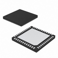
MAX19707ETM+ Maxim Integrated Products, MAX19707ETM+ Datasheet - Page 29

MAX19707ETM+
Manufacturer Part Number
MAX19707ETM+
Description
IC ANLG FRONT END 45MSPS 48-TQFN
Manufacturer
Maxim Integrated Products
Datasheet
1.MAX19707ETM.pdf
(37 pages)
Specifications of MAX19707ETM+
Number Of Bits
10
Number Of Channels
4
Power (watts)
84.6mW
Voltage - Supply, Analog
3V
Voltage - Supply, Digital
3V
Package / Case
48-TQFN Exposed Pad
Lead Free Status / RoHS Status
Lead free / RoHS Compliant
The MAX19707 features an internal precision 1.024V
bandgap reference that is stable over the entire power-
supply and temperature ranges. The REFIN input pro-
vides two modes of reference operation. The voltage at
REFIN (V
(Table 17).
In internal reference mode, connect REFIN to V
V
REFP, and REFN are low-impedance outputs with
V
V
COM each with a 0.33µF capacitor. Bypass REFIN to
GND with a 0.1µF capacitor.
In buffered external reference mode, apply 1.024V
±10% at REFIN. In this mode, COM, REFP, and REFN
are low-impedance outputs with V
V
V
0.33µF capacitor. Bypass REFIN to GND with a 0.1µF
capacitor. In this mode, the Tx DAC full-scale output is
proportional to the external reference. For example, if
the V
scale output is also increased by 10% or ±440mV.
An RF transformer (Figure 8) provides an excellent
solution to convert a single-ended signal source to a
fully differential signal for optimum ADC performance.
Connecting the center tap of the transformer to COM
provides a V
transformer can be used, or a step-up transformer can
be selected to reduce the drive requirements. In gener-
al, the MAX19707 provides better SFDR and THD with
fully differential input signals than single-ended signals,
Table 17. Reference Modes
REF
COM
REFN
REFP
REFIN
1.024V ±10%
> 0.8V x V
REFIN
is an internally generated 0.512V ±4%. COM,
V
Using Balun Transformer AC-Coupling
= V
= V
= V
/ 4. Bypass REFP, REFN, and COM each with a
REFIN
REFIN
DD
DD
DD
is increased by 10% (max), the Tx DAC full-
DD
DD
/ 2 + V
/ 2 - V
/ 2, V
Applications Information
) sets the reference operation mode
/ 2 DC level shift to the input. A 1:1
______________________________________________________________________________________
Internal Reference Mode. V
with a 0.33µF capacitor.
Buffered External Reference Mode. An external 1.024V ±10% reference voltage is applied to REFIN. V
internally generated to be V
REFIN to GND with a 0.1µF capacitor.
REFP
REF
REFIN
Reference Configurations
/ 2. Bypass REFP, REFN, and
= V
/ 4, and V
DD
/ 2 + V
10-Bit, 45Msps, Ultra-Low-Power
REFN
COM
REF
REF
= V
= V
REFIN
/ 2, and
is internally generated to be 0.512V. Bypass REFP, REFN, and COM each
DD
DD
/ 2. Bypass REFP, REFN, and COM each with a 0.33µF capacitor. Bypass
/ 2 -
/ 2,
DD
.
REFERENCE MODE
especially for high input frequencies. In differential
mode, even-order harmonics are lower as both inputs
(IAP, IAN, QAP, QAN) are balanced, and each of the
Rx ADC inputs only requires half the signal swing com-
pared to single-ended mode. Figure 9 shows an RF
transformer converting the MAX19707 Tx DAC differen-
tial analog outputs to single-ended.
Figure 8. Balun Transformer-Coupled Single-Ended-to-
Differential Input Drive for Rx ADC
V
V
IN
IN
0.1μF
0.1μF
Analog Front-End
0.33μF
0.33μF
25Ω
25Ω
25Ω
25Ω
0.1μF
0.1μF
22pF
22pF
22pF
22pF
IAP
COM
IAN
QAP
QAN
MAX19707
REF
is
29


