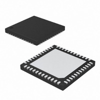
MAX5864ETM+ Maxim Integrated Products, MAX5864ETM+ Datasheet - Page 12

MAX5864ETM+
Manufacturer Part Number
MAX5864ETM+
Description
IC ANLG FRONT END 22MSPS 48-TQFN
Manufacturer
Maxim Integrated Products
Datasheet
1.MAX5864ETM.pdf
(26 pages)
Specifications of MAX5864ETM+
Number Of Bits
10
Number Of Channels
4
Power (watts)
2.10W
Voltage - Supply, Analog
2.7 V ~ 3.3 V
Voltage - Supply, Digital
1.8 V ~ 3.3 V
Package / Case
48-TQFN Exposed Pad
Lead Free Status / RoHS Status
Lead free / RoHS Compliant
Ultra-Low-Power, High Dynamic-
Performance, 22Msps Analog Front End
12
13–16, 19–22
5, 7, 12, 37,
11, 33, 39
2, 8, 43
40, 41
44, 45
23–32
______________________________________________________________________________________
PIN
42
10
17
18
34
35
36
38
46
47
48
—
1
3
4
6
9
QD+, QD-
DA0–DA7
DD0–DD9
ID-, ID+
OGND
NAME
REFIN
OV
REFP
SCLK
REFN
COM
GND
QA+
CLK
N.C.
V
QA-
V
DIN
IA+
IA-
CS
EP
DD
DD
DD
Upper Reference Voltage. Bypass with a 0.33µF capacitor to GND as close to REFP as possible.
Analog Supply Voltage. Bypass V
0.1µF capacitor.
Channel IA Positive Analog Input. For single-ended operation, connect signal source to IA+.
Channel IA Negative Analog Input. For single-ended operation, connect IA- to COM.
Analog Ground. Connect all pins to GND ground plane.
Conversion Clock Input. Clock signal for both ADCs and DACs.
Channel QA Negative Analog Input. For single-ended operation, connect QA- to COM.
Channel QA Positive Analog Input. For single-ended operation, connect signal source to QA+.
Analog Supply Voltage. Connect to V
ADC Tri-State Digital Output Bits. DA7 is the most significant bit (MSB), and DA0 is the least
significant bit (LSB).
Output Driver Ground
Output Driver Power Supply. Supply range from +1.8V to V
Bypass OV
DAC Digital Input Bits. DD9 is the MSB, and DD0 is the LSB.
3-Wire Serial Interface Data Input. Data is latched on the rising edge of the SCLK.
3-Wire Serial Interface Clock Input
3-Wire Serial Interface Chip Select Input. Apply logic low enables the serial interface.
No Connection
DAC Channel-QD Differential Voltage Output
DAC Channel-ID Differential Voltage Output
Reference Input. Connect to V
Common-Mode Voltage I/O. Bypass COM to GND with a 0.33µF capacitor.
Negative Reference I/O. Conversion range is ±(V
capacitor.
Exposed Paddle. Exposed paddle is internally connected to GND. Connect EP to the GND plane.
DD
to OGND with a combination of a 2.2µF capacitor in parallel with a 0.1µF capacitor.
DD
DD
for internal reference.
to GND with a combination of a 2.2µF capacitor in parallel with a
DD
power plane as close to the device as possible.
FUNCTION
REFP
- V
REFN
DD
). Bypass REFN to GND with a 0.33µF
to accommodate most logic levels.
Pin Description


