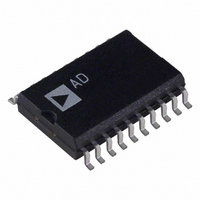
AD73311LAR Analog Devices Inc, AD73311LAR Datasheet - Page 18

AD73311LAR
Manufacturer Part Number
AD73311LAR
Description
IC ANALOG FRONT END 20-SOIC
Manufacturer
Analog Devices Inc
Datasheet
1.AD73311LAR.pdf
(36 pages)
Specifications of AD73311LAR
Rohs Status
RoHS non-compliant
Number Of Bits
16
Number Of Channels
2
Power (watts)
50mW
Voltage - Supply, Analog
3V
Voltage - Supply, Digital
3V
Package / Case
20-SOIC (7.5mm Width)
Single Supply Voltage (min)
2.7V
Single Supply Voltage (max)
3.3V
Package Type
SOIC W
Lead Free Status / RoHS Status
Not Compliant
Available stocks
Company
Part Number
Manufacturer
Quantity
Price
Part Number:
AD73311LAR
Manufacturer:
ADI/亚德诺
Quantity:
20 000
Company:
Part Number:
AD73311LARS
Manufacturer:
AD
Quantity:
12
Part Number:
AD73311LARS
Manufacturer:
ADI/亚德诺
Quantity:
20 000
Company:
Part Number:
AD73311LARS/AD73311
Manufacturer:
LITEON
Quantity:
10 000
Company:
Part Number:
AD73311LARSREEL
Manufacturer:
STM
Quantity:
6 706
Company:
Part Number:
AD73311LARSZ
Manufacturer:
MIC
Quantity:
6 222
Part Number:
AD73311LARSZ
Manufacturer:
ADI/亚德诺
Quantity:
20 000
Part Number:
AD73311LARSZ-REEL
Manufacturer:
ADI/亚德诺
Quantity:
20 000
Part Number:
AD73311LARU
Manufacturer:
ADI/亚德诺
Quantity:
20 000
INTERFACING
The AD73311L can be interfaced to most modern DSP engines
using conventional serial port connections and an extra enable
control line. Both serial input and output data use an accompa-
nying frame synchronization signal which is active high one
clock cycle before the start of the 16-bit word or during the last
bit of the previous word if transmission is continuous. The serial
clock (SCLK) is an output from the codec and is used to define
the serial transfer rate to the DSP’s Tx and Rx ports. Two primary
configurations can be used: the first is shown in Figure 13, where
the DSP’s Tx data, Tx frame sync, Rx data and Rx frame sync
are connected to the codec’s SDI, SDIFS, SDO and SDOFS,
respectively. This configuration, referred to as indirectly coupled
or nonframe sync loop-back, has the effect of decoupling the
transmission of input data from the receipt of output data. The
delay between receipt of codec output data and transmission of
input data for the codec is determined by the DSP’s software
latency. When programming the DSP serial port for this con-
figuration, it is necessary to set the Rx F
F
most useful when operating in mixed mode, as the DSP has the
ability to decide how many words (either DAC or control) can be
sent to the codec(s). This means that full control can be imple-
mented over the device configuration as well as updating the
DAC in a given sample interval. The second configuration
(shown in Figure 14) has the DSP’s Tx data and Rx data con-
nected to the codec’s SDI and SDO, respectively while the
DSP’s Tx and Rx frame syncs are connected to the codec’s
SDIFS and SDOFS. In this configuration, referred to as directly
coupled or frame sync loop-back, the frame sync signals are
connected together and the input data to the codec is forced to
be synchronous with the output data from the codec. The DSP
must be programmed so that both the Tx F
AD73311L
S
REFOUT
REFCAP
as an output generated by the DSP. This configuration is
VOUTN
VOUTP
VINN
VINP
LOOP-BACK
ANALOG
SELECT
+6/–15dB
PGA
REFERENCE
CONTINUOUS
LOW-PASS
FILTER
TIME
S
INVERT
as an input and the Tx
S
and Rx F
V
AD73311L
REF
SINGLE-
ENABLE
0/38dB
S
ENDED
PGA
are
inputs as the codec SDOFS will be input to both. This configura-
tion guarantees that input and output events occur simultaneously
and is the simplest configuration for operation in normal Data
Mode. Note that when programming the DSP in this configura-
tion it is advisable to preload the Tx register with the first control
word to be sent before the codec is taken out of reset. This
ensures that this word will be transmitted to coincide with the
first output word from the device(s).
Cascade Operation
The AD73311L has been designed to support up to eight codecs
in a cascade connected to a single serial port (see Figure 37).
The SPORT interface protocol has been designed so that device
addressing is built into the packet of information sent to the device.
This allows the cascade to be formed with no extra hardware
overhead for control signals or addressing. A cascade can be
formed in either of the two modes previously discussed.
There may be some restrictions in cascade operation due to the
number of devices configured in the cascade and the serial clock
rate chosen. Table XVII details the requirements for SCLK rate
for cascade lengths from 1 to 8 devices. This assumes a directly
coupled frame sync arrangement as shown in Figure 13.
SCLK
DMCLK
DMCLK/2
DMCLK/4
DMCLK/8
ADSP-218x
ADSP-218x
DSP
DSP
Table XVII. Cascade Options
1
TFS
DT
SCLK
RFS
TFS
DT
SCLK
RFS
DR
DR
Number of Devices in Cascade
2
3
X
4
X
SDOFS
SDOFS
SDIFS
SDIFS
SCLK
SCLK
SDO
SDO
SDI
SDI
5
X
X
AD73311L
AD73311L
CODEC
CODEC
6
X
X
7
X
X
8
X
X


