MCP3304-CI/SL Microchip Technology, MCP3304-CI/SL Datasheet - Page 15
MCP3304-CI/SL
Manufacturer Part Number
MCP3304-CI/SL
Description
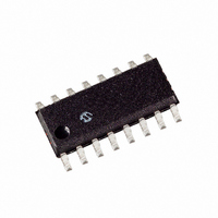
IC ADC 13BIT 2.7V 4CH SPI 16SOIC
Manufacturer
Microchip Technology
Specifications of MCP3304-CI/SL
Package / Case
16-SOIC (0.154", 3.90mm Width)
Number Of Bits
13
Sampling Rate (per Second)
100k
Data Interface
Serial, SPI™
Number Of Converters
1
Voltage Supply Source
Single Supply
Operating Temperature
-40°C ~ 85°C
Mounting Type
Surface Mount
Architecture
SAR
Conversion Rate
100 KSPs
Resolution
12 bit
Input Type
Voltage
Snr
80.02 dB
Maximum Operating Temperature
+ 85 C
Mounting Style
SMD/SMT
Minimum Operating Temperature
- 40 C
Lead Free Status / RoHS Status
Lead free / RoHS Compliant
Lead Free Status / RoHS Status
Lead free / RoHS Compliant, Lead free / RoHS Compliant
Other names
MCP3304CI/SL
Available stocks
Company
Part Number
Manufacturer
Quantity
Price
Company:

Part Number:
MCP3304-CI/SL
Manufacturer:
MICROCHIP
Quantity:
12 000
Part Number:
MCP3304-CI/SL
Manufacturer:
MICROCHIP/微芯
Quantity:
20 000


4.0
The descriptions of the pins are listed in Table 4-1.
TABLE 4-1:
4.1
Analog input channels. These pins have an absolute
voltage range of V
differential input range is defined as the absolute value
of (IN+) - (IN-). This difference can not exceed the
value of V
occur.
4.2
Ground connection to internal digital circuitry. To
ensure accuracy this pin must be connected to the
same ground as AGND. If an analog ground plane is
available, it is recommended that this device be tied to
the analog ground plane in the circuit. See Section 6.6
for more information regarding circuit layout.
4.3
The CS/SHDN pin is used to initiate communication
with the device when pulled low. This pin will end a con-
version and put the device in low power standby when
pulled high. The CS/SHDN pin must be pulled high
between conversions and cannot be tied low for multi-
ple conversions. See Figure 7-2 for serial communica-
tion protocol.
4.4
The SPI port serial data input pin is used to clock in
input channel configuration data. Data is latched on the
rising edge of the clock. See Figure 7-2 for serial com-
munication protocol.
4.5
The SPI serial data output pin is used to shift out the
results of the A/D conversion. Data will always change
on the falling edge of each clock as the conversion
takes place. See Figure 7-2 for serial communication
protocol.
CH0-CH7
DGND
CS/SHDN
D
D
CLK
AGND
V
V
2002 Microchip Technology Inc.
REF
DD
IN
OUT
Name
PIN DESCRIPTIONS
CH0-CH7
DGND
Chip Select/Shutdown (CS/SHDN)
Serial Data Input (D
Serial Data Output (D
REF
Analog Inputs
Digital Ground
Chip Select / Shutdown Input
Serial Data In
Serial Data Out
Serial Clock
Analog Ground
Reference Voltage Input
+2.7V to 5.5V Power Supply
- 1 LSB or digital code saturation will
SS
PIN FUNCTION TABLE
- 0.3V to V
Function
DD
+ 0.3V. The full scale
IN
)
OUT
)
4.6
The SPI clock pin is used to initiate a conversion and to
clock out each bit of the conversion as it takes place.
See Section 6.2 for constraints on clock speed. See
Figure 7-2 for serial communication protocol.
4.7
Ground connection to internal analog circuitry. To
ensure accuracy, this pin must be connected to the
same ground as DGND. If an analog ground plane is
available, it is recommended that this device be tied to
the analog ground plane in the circuit. See Section 6.6
for more information regarding circuit layout.
4.8
This input pin provides the reference voltage for the
device, which determines the maximum range of the
analog input signal and the LSB size.
The LSB size is determined according to the equation
shown below. As the reference input is reduced, the
LSB size is reduced accordingly.
EQUATION
When using an external voltage reference device, the
system designer should always refer to the manufac-
turer’s recommendations for circuit layout. Any instabil-
ity in the operation of the reference device will have a
direct effect on the accuracy of the ADC conversion
results.
4.9
The voltage on this pin can range from 2.7 to 5.5V. To
ensure accuracy, a 0.1 F ceramic bypass capacitor
should be placed as close as possible to the pin. See
Section 6.6 for more information regarding circuit lay-
out.
Serial Clock (CLK)
AGND
Voltage Reference (V
V
DD
LSB Size =
MCP3302/04
2 x V
8192
REF
REF
DS21697B-page 15
)
Related parts for MCP3304-CI/SL
Image
Part Number
Description
Manufacturer
Datasheet
Request
R

Part Number:
Description:
IC ADC 13BIT 2.7V 4CH SPI 16-DIP
Manufacturer:
Microchip Technology
Datasheet:
Part Number:
Description:
IC ADC 13BIT 2.7V 4CH SPI 16DIP
Manufacturer:
Microchip Technology
Datasheet:

Part Number:
Description:
ADC Single SAR 100KSPS 12-Bit+Sign Serial 16-Pin SOIC N Tube
Manufacturer:
Microchip Technology
Datasheet:
Part Number:
Description:
13-Bit Differential Input, Low Power A/D Converter with SPI Serial Interface
Manufacturer:
Microchip Technology
Datasheet:

Part Number:
Description:
Manufacturer:
Microchip Technology Inc.
Datasheet:
Part Number:
Description:
Manufacturer:
Microchip Technology Inc.
Datasheet:
Part Number:
Description:
Manufacturer:
Microchip Technology Inc.
Datasheet:
Part Number:
Description:
Manufacturer:
Microchip Technology Inc.
Datasheet:
Part Number:
Description:
Manufacturer:
Microchip Technology Inc.
Datasheet:
Part Number:
Description:
Manufacturer:
Microchip Technology Inc.
Datasheet:
Part Number:
Description:
Manufacturer:
Microchip Technology Inc.
Datasheet: