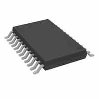
AD7367BRUZ-5 Analog Devices Inc, AD7367BRUZ-5 Datasheet - Page 19

AD7367BRUZ-5
Manufacturer Part Number
AD7367BRUZ-5
Description
IC ADC 14BIT DUAL 500KSPS 24-TSS
Manufacturer
Analog Devices Inc
Datasheet
1.AD7367BRUZ-5.pdf
(28 pages)
Specifications of AD7367BRUZ-5
Data Interface
DSP, MICROWIRE™, QSPI™, Serial, SPI™
Design Resources
Driving the AD7366/7 Bipolar SAR ADC in Low-Distortion DC-Coupled Appls (CN0042)
Number Of Bits
14
Sampling Rate (per Second)
500k
Number Of Converters
2
Power Dissipation (max)
88.8mW
Voltage Supply Source
Analog and Digital, Dual ±
Operating Temperature
-40°C ~ 85°C
Mounting Type
Surface Mount
Package / Case
24-TSSOP (0.173", 4.40mm Width)
Resolution (bits)
14bit
Input Channel Type
Single Ended
Supply Voltage Range - Analogue
4.75V To 5.25V, ± 11.5V To ± 16.5V
Supply Voltage Range - Digital
2.7V To
Sampling Rate
1MSPS
Rohs Compliant
Yes
Lead Free Status / RoHS Status
Lead free / RoHS Compliant
For Use With
EVAL-AD7367CBZ - BOARD EVALUATION FOR AD7367
Lead Free Status / RoHS Status
Lead free / RoHS Compliant, Lead free / RoHS Compliant
Available stocks
Company
Part Number
Manufacturer
Quantity
Price
Company:
Part Number:
AD7367BRUZ-5
Manufacturer:
ADI
Quantity:
1 000
Company:
Part Number:
AD7367BRUZ-5-RL7
Manufacturer:
ADI
Quantity:
1 000
+10V/+5V
DRIVER AMPLIFIER CHOICE
Each AD7366-5/AD7367-5 has a total of four analog inputs,
which operate in single-ended mode. Both ADC analog inputs
can be programmed to one of the three analog input ranges. In
applications where the signal source is high impedance, it is
recommended to buffer the signal before applying it to the
ADC analog inputs. Figure 21 shows the configuration of the
AD7366-5/AD7367-5 in single-ended mode.
In applications where the THD and SNR are critical specifi-
cations, the analog input of the AD7366-5/AD7367-5 should be
driven from a low impedance source. Large source impedances
significantly affect the ac performance of the ADC and can
necessitate the use of an input buffer amplifier.
When no amplifier is used to drive the analog input, the source
impedance should be limited to low values. The maximum source
impedance depends on the amount of THD that can be tolerated
in the application. The THD increases as the source impedance
increases and performance degrades. Figure 7 shows THD vs.
the analog input frequency for various source impedances.
Depending on the input range and analog input configuration
selected, the AD7366-5/AD7367-5 can handle source
impedances as illustrated in Figure 7.
Due to the programmable nature of the analog inputs on the
AD7366-5/AD7367-5, the choice of op amp used to drive the
inputs is a function of the particular application and depends
on the selected analog input voltage ranges.
The driver amplifier must be able to settle for a full-scale step to
a 14-bit level, 0.0061%, in less than the specified acquisition time
of the AD7366-5/AD7367-5. An op amp such as the
meets this requirement when operating in single-ended mode.
The AD8021 needs an external compensating NPO type of
capacitor. The
applications where a dual version is required. For lower frequency
applications, recommended op amps are the AD797, AD845,
and AD8610.
–10V/–5V
AGND
Figure 21. Typical Connection Diagram with the AD8021
Driving the Analog Input in Single-Ended Mode
AD8022
*ADDITIONAL PINS OMITTED FOR CLARITY.
can also be used in high frequency
1kΩ
AD8021
+
15pF
1kΩ
V+
V–
0.1µF
0.1µF
10µF
10µF
C
COMP
V
A1
AD7367-5*
AD7366-5/
= 10pF
V
DD
AD8021
V
SS
DV
CC
+5V
/AV
Rev. A | Page 19 of 28
CC
V
The AD7366-5/AD7367-5 also have a V
the voltage at which the serial interface operates. V
the ADC to easily interface to both 3 V and 5 V processors. For
example, if the AD7366-5/AD7367-5 is operated with a V
5 V, the V
a large dynamic range with low voltage digital processors. Thus,
the AD7366-5/AD7367-5 could be used with the ±10 V input
range while still being able to interface to 3 V digital parts.
REFERENCE
The AD7366-5/AD7367-5 can operate with either the internal
2.5 V on-chip reference or an externally applied reference. The
logic state of the REFSEL pin determines whether the internal
reference is used. The internal reference is selected for both ADCs
when the REFSEL pin is tied to logic high. If the REFSEL pin is
tied to GND, an external reference can be supplied through the
D
tied to either a low logic or high logic state for the part to operate.
Suitable reference sources for the AD7366-5/AD7367-5 include
the AD780, AD1582, ADR431, REF193, and ADR391.
The internal reference circuitry consists of a 2.5 V band gap
reference and a reference buffer. When operating the AD7366-5/
AD7367-5 in internal reference mode, the 2.5 V internal reference
is available at the D
decoupled to AGND using a 680 nF capacitor. It is recommended
that the internal reference be buffered before applying it elsewhere
in the system. The internal reference is capable of sourcing up
to 150 μA with an analog input range of ±10 V and 70 μA for
both the ±5 V range and 0 V to +10 V range
If the internal reference operation is required for the ADC
conversion, the REFSEL pin must be tied to logic high on power-
up. The reference buffer requires 70 μs to power up and charge
the 680 nF decoupling capacitor during the power-up time.
The AD7366-5/AD7367-5 is specified for a 2.5 V to 3 V reference
range. When a 3 V reference is selected, the ranges are ±12 V,
±6 V, and 0 V to +12 V. For these ranges, the V
must be greater than or equal to the +12 V and −12 V, respectively.
DRIVE
CAP
A and D
DRIVE
CAP
pin could be powered from a 3 V supply, allowing
B pins. On power-up, the REFSEL pin must be
CAP
A and D
CAP
AD7366-5/AD7367-5
B pins, which should be
DRIVE
feature to control
DD
and V
DRIVE
SS
allows
supply
CC
of


