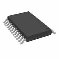
AD7367BRUZ-5 Analog Devices Inc, AD7367BRUZ-5 Datasheet - Page 21

AD7367BRUZ-5
Manufacturer Part Number
AD7367BRUZ-5
Description
IC ADC 14BIT DUAL 500KSPS 24-TSS
Manufacturer
Analog Devices Inc
Datasheet
1.AD7367BRUZ-5.pdf
(28 pages)
Specifications of AD7367BRUZ-5
Data Interface
DSP, MICROWIRE™, QSPI™, Serial, SPI™
Design Resources
Driving the AD7366/7 Bipolar SAR ADC in Low-Distortion DC-Coupled Appls (CN0042)
Number Of Bits
14
Sampling Rate (per Second)
500k
Number Of Converters
2
Power Dissipation (max)
88.8mW
Voltage Supply Source
Analog and Digital, Dual ±
Operating Temperature
-40°C ~ 85°C
Mounting Type
Surface Mount
Package / Case
24-TSSOP (0.173", 4.40mm Width)
Resolution (bits)
14bit
Input Channel Type
Single Ended
Supply Voltage Range - Analogue
4.75V To 5.25V, ± 11.5V To ± 16.5V
Supply Voltage Range - Digital
2.7V To
Sampling Rate
1MSPS
Rohs Compliant
Yes
Lead Free Status / RoHS Status
Lead free / RoHS Compliant
For Use With
EVAL-AD7367CBZ - BOARD EVALUATION FOR AD7367
Lead Free Status / RoHS Status
Lead free / RoHS Compliant, Lead free / RoHS Compliant
Available stocks
Company
Part Number
Manufacturer
Quantity
Price
Company:
Part Number:
AD7367BRUZ-5
Manufacturer:
ADI
Quantity:
1 000
Company:
Part Number:
AD7367BRUZ-5-RL7
Manufacturer:
ADI
Quantity:
1 000
SHUTDOWN MODE
Shutdown mode is intended for use in applications where slow
throughput rates are required. Shutdown mode is suited to
applications where a series of conversions performed at a
relatively high throughput rate are followed by a long period of
inactivity and, thus, shutdown. When the AD7366-5/AD7367-5
are in full power-down, all analog circuitry is powered down.
The falling edge of CNVST initiates the conversion. The BUSY
output subsequently goes high to indicate that the conversion is
in progress. Once the conversion is completed, the BUSY output
returns low. If the CNVST signal is at logic low when BUSY
goes low, the part enters shutdown at the end of the conversion
phase. While the part is in shutdown mode, the digital output
code from the last conversion on each ADC can still be read
from the D
low as described in the
return to three-state once
To exit full power-down and to power up the AD7366-5/
AD7367-5, a rising edge of CNVST is required. After the
required power-up time has elapsed, CNVST may be brought
low again to initiate another conversion, as shown in Figure 24
OUT
CNVST
BUSY
SCLK
pins. To read the D
CS
Serial Interface
CS
is brought back to logic high.
t
OUT
2
data,
section. The D
CS
must be brought
t
CONVERT
Figure 24. Autoshutdown Mode for AD7366-5
OUT
pins
ENTERS SHUTDOWN
Rev. A | Page 21 of 28
1
t
3
POWER-UP TIMES
As described in the Shutdown Mode section, the AD7366-5/
AD7367-5 have one power-down mode. This section deals with
the power-up time required when coming out of this mode. It
should be noted that these power-up times apply with the
recommended capacitors in place on the D
To power up from shutdown, CNVST must be brought high and
remain high for a minimum of 70 μs, as shown in
When power supplies are first applied to the AD7366-5/AD7367-5,
the ADC can power up with CNVST in either the low or high
logic state. Before attempting a valid conversion, CNVST must
be brought high and remain high for the recommended power-
up time of 70 μs. CNVST can then be brought low to initiate a
conversion. With the AD7366-5/AD7367-5, no dummy conversion
is required before valid data can be read from the
If it is intended to place the part in shutdown mode when the
supplies are first applied, the AD7366-5/AD7367-5 must be
powered up, and a conversion initiated. However, CNVST
should remain in the logic low state, and when the BUSY signal
goes low, the part enters shutdown.
Once supplies are applied to the AD7366-5/AD7367-5, sufficient
time must be allowed for any external reference to power up
and to charge the various reference buffer decoupling capacitors
to their final values.
12
SERIAL READ OPERATION
t
AD7366-5/AD7367-5
POWER-UP
CAP
A and D
D
Figure 24
OUT
CAP
pins.
B pins.
.


