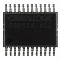
CS5524-ASZ Cirrus Logic Inc, CS5524-ASZ Datasheet - Page 46

CS5524-ASZ
Manufacturer Part Number
CS5524-ASZ
Description
IC ADC 24BIT 4CH 20SSOP
Manufacturer
Cirrus Logic Inc
Specifications of CS5524-ASZ
Number Of Converters
1
Package / Case
24-SSOP
Number Of Bits
24
Data Interface
Serial
Power Dissipation (max)
14.8mW
Voltage Supply Source
Analog and Digital
Operating Temperature
-40°C ~ 85°C
Mounting Type
Surface Mount
Number Of Adc Inputs
4
Architecture
Delta-Sigma
Conversion Rate
617 SPs
Resolution
24 bit
Input Type
Voltage
Interface Type
Serial (3-Wire)
Voltage Reference
2.5 V
Supply Voltage (max)
5 V
Supply Voltage (min)
25 mV
Maximum Power Dissipation
500 mW
Maximum Operating Temperature
+ 85 C
Mounting Style
SMD/SMT
Input Voltage
25 mV to 5 V
Minimum Operating Temperature
- 40 C
Lead Free Status / RoHS Status
Lead free / RoHS Compliant
For Use With
598-1012 - EVAL BOARD FOR CS5524 ADC
Lead Free Status / Rohs Status
Lead free / RoHS Compliant
Other names
598-1106-5
Available stocks
Company
Part Number
Manufacturer
Quantity
Price
Part Number:
CS5524-ASZ
Manufacturer:
CIRRUS
Quantity:
20 000
verter stays constant but the number of codes af-
fected is doubled because the code size has been
reduced by half.
The converter input ranges are specified with a
voltage reference of 2.5 V. The device can be op-
erated with the reference tied directly to the +5 V
supply. When this is done, the input span of the in-
put ranges is doubled; the 25 mV range actually be-
comes a 50 mV range. The gain register can be set
to 2.0 (shift contents left one bit) and the input
range will be scaled back to 25 mV. Since the gain
register can actually be as great as 4-2
one could scale the input span on the 25 mV range
to accept an analog full-scale span of about
6.25 mV. This is useful for ratiometric bridge mea-
surement of low-level differential outputs.
The gain register can also be scaled manually to a
value lower than 1.0. It is not recommended to use
the devices with the gain register scaled lower than
0.6. This can enable the converter to accept a
40 mV input signal on the 25 mV range when using
a voltage reference of 2.5 V. Caution though in
scaling the gain register below 1.0 on the 100 mV,
2.5 and 5 volt ranges as the analog signal path into
the converter may saturate before the expected
full-scale code output is produced by the converter.
Note that digital gain scaling will directly influence
the number of digital output codes affected by
noise. The effects can be analytically determined
by calculating the size of the codes (V/Count)
which result from a given gain scaling condition
and relating the amount of noise in the converter
relative to the determined code size. The evalua-
tion board for the converter is a useful tool to aid
the assessment of noise performance with various
voltage reference values, input range settings, and
gain register settings. The evaluation board sup-
ports noise analysis through data capture and noise
histogram analysis.
46
-22
decimal,
2.10 Getting Started
The CS5521/22/23/24/28 have many features.
From a software programmer’s perspective, what
should be done first? To begin, a 32.768 kHz crys-
tal takes approximately 500 ms to start-up. To ac-
commodate for this, it is recommended that a
software delay of approximately 500 ms to 1 sec-
ond precede the processor’s ADC initialization
code before any registers are accessed in the ADC.
This delay time is dependent on the start-up delay
of the clock source. If a CMOS clock source with
no start-up delay is being used to drive the ADC,
then this delay is not necessary.
The converters include an on-chip, power-on reset
circuit to automatically reset the ADCs shortly af-
ter
CS5521/22/23/24/28 is applied, the chips are held
in a reset condition until the 32.768 kHz oscillator
has started and a counter-timer elapses. The
counter-timer counts 2006 oscillator clock cycles
to make sure the oscillator is fully stable. During
this time-out period the serial port logic is reset and
the RV (Reset Valid) bit in the configuration regis-
ter is set to indicate that a valid reset occurred. In
normal start-up conditions, this power-on-reset cir-
cuit should reset the chip when power is applied. If
your application may experience abnormal power
start-up conditions, the following sequence of in-
structions should be performed to guarantee the
converter begins proper operation:
1) After power is applied, initialize the serial port
2) Write a ‘1’ to the reset bit (RS) of the configu-
3) Read the configuration register to determine if
4) When the RV bit has been set to ‘1’, reset the
using the serial port synchronization sequence.
ration register to reset the converter.
the reset valid bit (RV) is set to ‘1’. If the RV
bit is not set, the configuration register should
be read again.
RS bit back to ‘0’ by writing to 0x000000 to the
power
up.
CS5521/22/23/24/28
When
power
DS317F4
to
the


