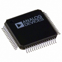
AD7658BSTZ Analog Devices Inc, AD7658BSTZ Datasheet - Page 4

AD7658BSTZ
Manufacturer Part Number
AD7658BSTZ
Description
IC ADC 12BIT 6CH 250KSPS 64LQFP
Manufacturer
Analog Devices Inc
Datasheet
1.AD7656BSTZ-500RL7.pdf
(32 pages)
Specifications of AD7658BSTZ
Data Interface
Serial, Parallel
Number Of Bits
12
Sampling Rate (per Second)
250k
Number Of Converters
6
Power Dissipation (max)
143mW
Voltage Supply Source
Analog and Digital, Dual ±
Operating Temperature
-40°C ~ 85°C
Mounting Type
Surface Mount
Package / Case
64-LQFP
Resolution (bits)
12bit
Sampling Rate
250kSPS
Input Channel Type
Single Ended
Supply Voltage Range - Digital
4.75V To 5.25V
Supply Current
26mA
Lead Free Status / RoHS Status
Lead free / RoHS Compliant
For Use With
EVAL-AD7658CBZ - BOARD EVAL FOR AD7658
Lead Free Status / RoHS Status
Lead free / RoHS Compliant, Lead free / RoHS Compliant
Available stocks
Company
Part Number
Manufacturer
Quantity
Price
Company:
Part Number:
AD7658BSTZ
Manufacturer:
ADI
Quantity:
329
Company:
Part Number:
AD7658BSTZ
Manufacturer:
Analog Devices Inc
Quantity:
10 000
Part Number:
AD7658BSTZ
Manufacturer:
ADI/亚德诺
Quantity:
20 000
Company:
Part Number:
AD7658BSTZ-1
Manufacturer:
Analog Devices Inc
Quantity:
10 000
Company:
Part Number:
AD7658BSTZ-1-RL
Manufacturer:
Analog Devices Inc
Quantity:
10 000
Company:
Part Number:
AD7658BSTZ-REEL
Manufacturer:
Analog Devices Inc
Quantity:
10 000
AD7656/AD7657/AD7658
Parameter
LOGIC INPUTS
LOGIC OUTPUTS
CONVERSION RATE
POWER REQUIREMENTS
1
2
3
Temperature ranges are as follows: B version is −40°C to +85°C and Y version is −40°C to +125°C.
See the Terminology section.
Sample tested during initial release to ensure compliance.
Input High Voltage (V
Input Low Voltage (V
Input Current (I
Input Capacitance (C
Output High Voltage (V
Output Low Voltage (V
Floating-State Leakage Current
Floating-State Output Capacitance
Output Coding
Conversion Time
Track-and-Hold Acquisition Time
Throughput Rate
V
V
AV
DV
V
I
I
I
Power Dissipation
TOTAL
SS
DD
DD
SS
DRIVE
Normal Mode (Static)
Normal Mode (Operational)
(Operational)
Partial Power-Down Mode
Full Power-Down Mode (STBY Pin)
Normal Mode (Static)
Normal Mode (Operational)
Partial Power-Down Mode
Full Power-Down Mode (STBY Pin)
CC
(Operational)
CC
(Includes IAV
(Includes IAV
IN
)
CC
CC
, IV
, IV
IN
INL
INH
)
OL
DD
DD
3
)
OH
)
)
, IV
, IV
)
SS
SS
, IV
, IV
DRIVE
DRIVE
2, 3
3
, IDV
, IDV
CC
CC
)
)
B Version
0.7 × V
0.3 × V
±1
10
V
0.2
±1
10
3.1
550
250
5/15
−5/−15
5
5
3/5
28
26
0.25
0.25
7
80
143
140
35
100
DRIVE
Twos complement
− 0.2
DRIVE
DRIVE
1
Rev. A | Page 4 of 32
Y Version
0.7 × V
0.3 × V
±1
10
V
0.2
±1
10
3.1
550
250
5/15
−5/−15
5
5
3/5
28
26
0.25
0.25
7
80
143
140
35
100
DRIVE
− 0.2
DRIVE
DRIVE
1
pF max
V max
pF max
μs max
ns max
kSPS
V nom
V nom
mA max
mA max
μA max
mW max
mW max
μW max
Unit
V min
V max
μA max
V min
μA max
V nom min/max
V nom min/max
V nom min/max
mA max
mA max
mA max
mW max
Test Conditions/Comments
Typically 10 nA, V
I
I
Parallel interface mode only
For 4 × V
For 4 × V
Digital I/P
AV
V
f
V
V
V
AV
V
SCLK on or off, AV
V
AV
V
f
SOURCE
SINK
SAMPLE
SAMPLE
SS
DD
SS
DD
SS
DD
SS
CC
CC
CC
= −16.5 V
= −16.5 V, f
= −16.5 V
= −16.5 V
= 16.5 V, V
= 16.5 V, f
= 16.5 V, V
= 200 μA
= DV
= DV
= DV
= 250 kSPS, AV
= 200 μA
= 250 kSPS
REF
REF
CC
S
CC
CC
= 0 V or V
range, V
range, V
= V
= V
= V
SAMPLE
SS
SS
SAMPLE
DRIVE
DRIVE
DRIVE
= −16.5 V
= −16.5 V
IN
CC
= 250 kSPS
= 5.25 V, V
= 0 V or V
= 5.25 V, V
= 5.25 V, V
DD
DD
CC
= 250 kSPS
= DV
DRIVE
= DV
= 10 V to 16.5 V
= −10 V to −16.5 V
CC
CC
= V
DRIVE
= V
DD
DD
DD
DRIVE
DRIVE
= 16.5 V,
= 16.5 V,
= 16.5 V,
= 5.25 V,
= 5.25 V,


