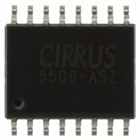
CS5509-ASZ Cirrus Logic Inc, CS5509-ASZ Datasheet - Page 11

CS5509-ASZ
Manufacturer Part Number
CS5509-ASZ
Description
IC ADC 16BIT SGNL SUPP 16-SOIC
Manufacturer
Cirrus Logic Inc
Datasheet
1.CS5509-ASZ.pdf
(24 pages)
Specifications of CS5509-ASZ
Number Of Converters
1
Package / Case
16-SOIC (0.300", 7.50mm Width)
Number Of Bits
16
Sampling Rate (per Second)
200
Data Interface
Serial
Power Dissipation (max)
2.25mW
Voltage Supply Source
Analog and Digital
Operating Temperature
-40°C ~ 85°C
Mounting Type
Surface Mount
Number Of Adc Inputs
1
Architecture
Delta-Sigma
Conversion Rate
20 SPs
Resolution
16 bit
Input Type
Voltage
Interface Type
Serial
Voltage Reference
1.2 V
Supply Voltage (max)
5 V
Supply Voltage (min)
3.3 V
Maximum Power Dissipation
2.25 mW
Maximum Operating Temperature
+ 85 C
Mounting Style
SMD/SMT
Input Voltage
3.3 V to 5 V
Minimum Operating Temperature
- 40 C
Lead Free Status / RoHS Status
Lead free / RoHS Compliant
Lead Free Status / RoHS Status
Lead free / RoHS Compliant, Lead free / RoHS Compliant
Other names
598-1100-5
Available stocks
Company
Part Number
Manufacturer
Quantity
Price
Company:
Part Number:
CS5509-ASZ
Manufacturer:
CIRRUS
Quantity:
44
Part Number:
CS5509-ASZ
Manufacturer:
CIRRUS
Quantity:
20 000
put signals. The converter can be used to convert
both unipolar and bipolar signals by changing the
BP/UP pin. Recalibration is not required when
switching between unipolar and bipolar modes.
At the end of the calibration cycle, the on-chip mi-
crocontroller checks the logic state of the CONV
signal. If the CONV input is low the device will en-
ter the standby mode where it waits for further in-
struction. If the CONV signal is high at the end of
the calibration cycle, the converter will enter the
conversion state and perform a conversion on the
input channel. The CAL signal can be returned low
any time after calibration is initiated. CONV can
also be returned low, but it should never be taken
low and then taken back high until the calibration
period has ended and the converter is in the standby
state. If CONV is taken low and then high again
with CAL high while the converter is calibrating,
the device will interrupt the current calibration cy-
cle and start a new one. If CAL is taken low and
CONV is taken low and then high during calibra-
tion, the calibration cycle will continue as the con-
version command is disregarded. The state of
BP/UP is not important during calibrations.
If an "end of calibration" signal is desired, pulse the
CAL signal high while leaving the CONV signal
high continuously. Once the calibration is complet-
ed, a conversion will be performed. At the end of
the conversion, DRDY will fall to indicate the first
valid conversion after the calibration has been
completed.
Conversion
The conversion state can be entered at the end of
the calibration cycle, or whenever the converter is
idle in the standby mode. If CONV is taken high to
initiate a calibration cycle ( CAL also high), and re-
mains high until the calibration cycle is completed
(CAL is taken low after CONV transitions high),
the converter will begin a conversion upon comple-
tion of the calibration period.
DS125F3
The BP/UP pin is not a latched input. The BP/UP
pin controls how the output word from the digital
filter is processed. In bipolar mode the output word
computed by the digital filter is offset by 8000H
(see Understanding Converter Calibration). BP/UP
can be changed after a conversion is started as long
as it is stable for 82 clock cycles of the conversion
period prior to DRDY falling. If one wishes to in-
termix measurement of bipolar and unipolar signals
on various input signals, it is best to switch the
BP/UP pin immediately after DRDY falls and
leave BP/UP stable until DRDY falls again.
The digital filter in the CS5509 has a Finite Im-
pulse Response and is designed to settle to full ac-
curacy in one conversion time.
If CONV is left high, the CS5509 will perform con-
tinuous conversions. The conversion time will be
1622 clock cycles. If conversion is initiated from
the standby state, there may be up to two XIN clock
cycles of uncertainty as to when conversion actual-
ly begins. This is because the internal logic oper-
ates at one half the external clock rate and the exact
phase of the internal clock may be 180° out of
phase relative to the XIN clock. When a new con-
version is initiated from the standby state, it will
take up to two XIN clock cycles to begin. Actual
conversion will use 1624 clock cycles before
DRDY goes low to indicate that the serial port has
been updated. See the Serial Interface Logic sec-
tion of the data sheet for information on reading
data from the serial port.
In the event the A/D conversion command (CONV
going positive) is issued during the conversion
state, the current conversion will be terminated and
a new conversion will be initiated.
Voltage Reference
The CS5509 uses a differential voltage reference
input. The positive input is VREF+ and the nega-
tive input is VREF-. The voltage between VREF+
and VREF- can range from 1 volt minimum to 3.6
volts maximum. The gain slope will track changes
CS5509
11


