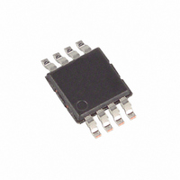
MAX11646EUA+ Maxim Integrated Products, MAX11646EUA+ Datasheet

MAX11646EUA+
Specifications of MAX11646EUA+
Related parts for MAX11646EUA+
MAX11646EUA+ Summary of contents
Page 1
... Power-Down Mode ♦ Software-Configurable Unipolar/Bipolar Ordering Information PART TEMP RANGE MAX11646EUA+ -40°C to +85°C 8 μMAX MAX11647EUA+ -40°C to +85°C 8 μMAX MAX11647EWC+ -40°C to +85°C 12 WLP + Denotes a lead(Pb)-free/RoHs-compliant package. Features DD 2 ...
Page 2
Low-Power, 1-/2-Channel Ultra-Tiny 1.9mm x 2.2mm Package ABSOLUTE MAXIMUM RATINGS V to GND ..............................................................-0.3V to +6V DD AIN0, AIN1, REF to GND ............-0.3V to the lower of (V SDA, SCL to GND.....................................................-0.3V to +6V Maximum Current Into Any ...
Page 3
Low-Power, 1-/2-Channel Ultra-Tiny 1.9mm x 2.2mm Package ELECTRICAL CHARACTERISTICS (continued 2.7V to 3.6V (MAX11647 1.7MHz unless otherwise noted. Typical values are at T SCL A ...
Page 4
Low-Power, 1-/2-Channel Ultra-Tiny 1.9mm x 2.2mm Package ELECTRICAL CHARACTERISTICS (continued 2.7V to 3.6V (MAX11647 1.7MHz unless otherwise noted. Typical values are at T SCL A ...
Page 5
Low-Power, 1-/2-Channel Ultra-Tiny 1.9mm x 2.2mm Package TIMING CHARACTERISTICS (Figure 1) (continued 2.7V to 3.6V (MAX11647 1.7MHz unless otherwise noted. Typical values are at T ...
Page 6
Low-Power, 1-/2-Channel Ultra-Tiny 1.9mm x 2.2mm Package (V = 3.3V (MAX11647 (MAX11646 +25°C, unless otherwise noted.) A DIFFERENTIAL NONLINEARITY vs. DIGITAL OUTPUT CODE 0.3 0.2 0.1 0 -0.1 -0.2 -0.3 ...
Page 7
Low-Power, 1-/2-Channel Ultra-Tiny 1.9mm x 2.2mm Package (V = 3.3V (MAX11647 (MAX11646 +25°C, unless otherwise noted.) A NORMALIZED REFERENCE VOLTAGE vs. SUPPLY VOLTAGE 1.00010 1.00008 1.00006 1.00004 1.00002 1.00000 0.99998 ...
Page 8
Low-Power, 1-/2-Channel Ultra-Tiny 1.9mm x 2.2mm Package TOP VIEW + AIN0 1 AIN1 2 MAX11646 MAX11647 N.C. 3 REF 4 µMAX PIN NAME μMAX WLP 1,2 A1, A2 AIN0, AIN1 3 — ...
Page 9
Low-Power, 1-/2-Channel Ultra-Tiny 1.9mm x 2.2mm Package A. F/S-MODE 2-WIRE SERIAL-INTERFACE TIMING SDA t SU:DAT t LOW SCL t t HD:STA HIGH HS-MODE 2-WIRE SERIAL-INTERFACE TIMING SDA t SU:DAT t LOW SCL t t ...
Page 10
Low-Power, 1-/2-Channel Ultra-Tiny 1.9mm x 2.2mm Package SDA SCL INPUT SHIFT REGISTER V DD GND CONFIGURATION REGISTER AIN0 AIN1 ANALOG REF INPUT MUX Figure 2. Functional Diagram SDA I OH Figure 3. Load Circuit ...
Page 11
Low-Power, 1-/2-Channel Ultra-Tiny 1.9mm x 2.2mm Package During the conversion interval, the switched capacitive DAC adjusts to restore the comparator input voltage to 0V within the limits of 10-bit resolution. This action requires 10 conversion clock cycles and ...
Page 12
Low-Power, 1-/2-Channel Ultra-Tiny 1.9mm x 2.2mm Package Single-Ended/Differential Input The SGL/DIF of the configuration byte configures the MAX11646/MAX11647 analog input circuitry for single- ended or differential inputs (Table 2). In single-ended mode (SGL/DIF = 1), the digital conversion ...
Page 13
Low-Power, 1-/2-Channel Ultra-Tiny 1.9mm x 2.2mm Package DEVICE MAX11646/MAX11647 SDA 1 SCL Figure 7. Slave Address Byte A bus master initiates communication with a slave device by issuing a START condition followed by a slave ...
Page 14
Low-Power, 1-/2-Channel Ultra-Tiny 1.9mm x 2.2mm Package Configuration/Setup Bytes (Write Cycle) A write cycle begins with the bus master issuing a START condition followed by 7 address bits (Figure 7) and a write bit (R/W = 0). If ...
Page 15
Low-Power, 1-/2-Channel Ultra-Tiny 1.9mm x 2.2mm Package Table 2. Configuration Byte Format BIT 7 BIT 6 BIT 5 (MSB) REG SCAN1 SCAN0 BIT NAME 7 REG Register bit. 1= setup byte (see Table 1 configuration byte. ...
Page 16
Low-Power, 1-/2-Channel Ultra-Tiny 1.9mm x 2.2mm Package When configured for internal clock mode (CLK = 0), the MAX11646/MAX11647 use their internal oscillator as the conversion clock. In internal clock mode, the MAX11646/MAX11647 begin tracking the analog input after ...
Page 17
Low-Power, 1-/2-Channel Ultra-Tiny 1.9mm x 2.2mm Package When configured for external clock mode (CLK = 1), the MAX11646/MAX11647 use the SCL as the conver- sion clock. In external clock mode, the MAX11646/ MAX11647 begin tracking the analog input ...
Page 18
Low-Power, 1-/2-Channel Ultra-Tiny 1.9mm x 2.2mm Package Applications Information The configuration and setup registers (Tables 1 and 2) default to a single-ended, unipolar, single-channel conver- sion on AIN0 using the internal clock with V ence. The memory contents ...
Page 19
Low-Power, 1-/2-Channel Ultra-Tiny 1.9mm x 2.2mm Package Transfer Functions Output data coding for the MAX11646/MAX11647 is binary in unipolar mode and two’s complement in bipo- N lar mode with 1 LSB = ( where N is ...
Page 20
Low-Power, 1-/2-Channel Ultra-Tiny 1.9mm x 2.2mm Package Differential Nonlinearity Differential nonlinearity (DNL) is the difference between an actual step width and the ideal value of 1 LSB. A DNL error specification of less than 1 LSB guarantees no ...
Page 21
Low-Power, 1-/2-Channel Ultra-Tiny 1.9mm x 2.2mm Package Typical Operating Circuit 3. 0.1μ SDA AIN0 ANALOG MAX11646 INPUTS AIN1 SCL MAX11647 RC NETWORK* 2kΩ REF GND C REF 0.1μ SDA μC SCL *OPTIONAL ...
Page 22
... Maxim cannot assume responsibility for use of any circuitry other than circuitry entirely embodied in a Maxim product. No circuit patent licenses are implied. Maxim reserves the right to change the circuitry and specifications without notice at any time. 22 ____________________Maxim Integrated Products, 120 San Gabriel Drive, Sunnyvale, CA 94086 408-737-7600 © 2010 Maxim Integrated Products ...


