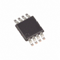
MAX11646EUA+ Maxim Integrated Products, MAX11646EUA+ Datasheet - Page 15

MAX11646EUA+
Manufacturer Part Number
MAX11646EUA+
Description
IC ADC 10BIT I2C 94.4KSPS 8UMAX
Manufacturer
Maxim Integrated Products
Datasheet
1.MAX11646EUA.pdf
(22 pages)
Specifications of MAX11646EUA+
Number Of Bits
10
Sampling Rate (per Second)
94.4k
Data Interface
I²C, Serial
Number Of Converters
1
Power Dissipation (max)
362mW
Voltage Supply Source
Single Supply
Operating Temperature
-40°C ~ 85°C
Mounting Type
Surface Mount
Package / Case
8-TSSOP, 8-MSOP (0.118", 3.00mm Width)
Number Of Adc Inputs
2
Conversion Rate
1 Ksps to 94.4 Ksps
Resolution
10 bit
Input Type
Single-Ended
Interface Type
I2C
Snr
60 dB
Voltage Reference
Internal 4.096 V
Supply Voltage (max)
5.5 V
Supply Voltage (min)
4.5 V
Maximum Power Dissipation
362 mW
Maximum Operating Temperature
+ 85 C
Input Voltage
4.5 V to 5.5 V
Minimum Operating Temperature
- 40 C
Lead Free Status / RoHS Status
Lead free / RoHS Compliant
A read cycle must be initiated to obtain conversion
results. Read cycles begin with the bus master issuing
a START condition followed by 7 address bits and a
read bit (R/W = 1). If the address byte is successfully
received, the MAX11646/MAX11647 (slave) issue an
acknowledge. The master then reads from the slave.
The result is transmitted in 2 bytes; first 6 bits of the first
byte are high, then MSB through LSB are consecutively
clocked out. After the master has received the byte(s),
it can issue an acknowledge if it wants to continue
reading or a not-acknowledge if it no longer wishes to
read. If the MAX11646/MAX11647 receive a not-
Table 2. Configuration Byte Format
X = Don’t care.
Table 3. Channel Selection in Single-
Ended Mode (SGL/DIF = 1)
X = Don’t care.
(MSB)
BIT 7
CS0
REG
BIT
0
1
7
6
5
4
3
2
1
0
Low-Power, 1-/2-Channel, I
SGL/
______________________________________________________________________________________
SCAN1
SCAN1
SCAN0
AIN0
NAME
BIT 6
REG
CS0
+
X
X
X
in Ultra-Tiny 1.9mm x 2.2mm Package
Register bit. 1= setup byte (see Table 1), 0 = configuration byte.
Scan-select bits. Two bits select the scanning configuration (Table 5). Defaults to 00 at power-up.
Channel-select bit. CS0 selects which analog input channels are to be used for conversion
(Tables 3 and 4). Defaults to 0000 at power-up.
1 = single-ended, 0 = differential (Tables 3 and 4). Defaults to 1 at power-up. See the Single-
Ended/Differential Input section.
Data Byte (Read Cycle)
AIN1
SCAN0
BIT 5
+
GND
-
-
BIT 4
X
acknowledge, they release SDA, allowing the master to
generate a STOP or a repeated START condition. See
the Clock Modes and Scan Mode sections for detailed
information on how data is obtained and converted.
The clock mode determines the conversion clock and
the data acquisition and conversion time. The clock
mode also affects the scan mode. The state of the set-
up byte’s CLK bit determines the clock mode (Table 1).
At power-up, the MAX11646/MAX11647 are defaulted
to internal clock mode (CLK = 0).
Table 4. Channel Selection in Differential
Mode (SGL/DIF = 0)
X = Don’t care.
BIT 3
X
DESCRIPTION
CS0
0
1
BIT 2
2
X
C, 10-Bit ADCs
AIN0
+
-
BIT 1
CS0
Clock Modes
AIN1
SGL/
+
(LSB)
BIT 0
-
15


