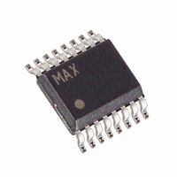
MAX11603EEE+ Maxim Integrated Products, MAX11603EEE+ Datasheet - Page 11

MAX11603EEE+
Manufacturer Part Number
MAX11603EEE+
Description
IC ADC SERIAL 8BIT 8CH 16-QSOP
Manufacturer
Maxim Integrated Products
Datasheet
1.MAX11602EEE.pdf
(23 pages)
Specifications of MAX11603EEE+
Number Of Bits
8
Sampling Rate (per Second)
188k
Data Interface
I²C, Serial
Number Of Converters
1
Power Dissipation (max)
1.75mW
Voltage Supply Source
Single Supply
Operating Temperature
-40°C ~ 85°C
Mounting Type
Surface Mount
Package / Case
16-SSOP (0.150", 3.90mm Width)
Resolution
8 bit
Interface Type
I2C
Snr
49 dB
Voltage Reference
2.048 V
Supply Voltage (max)
3.6 V
Supply Voltage (min)
2.7 V
Maximum Power Dissipation
666.7 mW
Maximum Operating Temperature
+ 85 C
Mounting Style
SMD/SMT
Input Voltage
3.3 V
Minimum Operating Temperature
- 40 C
Lead Free Status / RoHS Status
Lead free / RoHS Compliant
The SGL/DIF bit of the configuration byte configures the
MAX11600–MAX11605 analog input circuitry for single-
ended or pseudo-differential inputs (Table 2). In single-
ended mode (SGL/DIF = 1), the digital conversion results
are the difference between the analog input selected by
CS[3:0] and GND (Table 3). In pseudo-differential mode
(SGL/DIF = 0), the digital conversion results are the differ-
ence between the positive and the negative analog inputs
selected by CS[3:0] (Table 4). The negative analog input
signal must remain stable within ±0.5 LSB (±0.1 LSB for
best results) with respect to GND during a conversion.
When operating in pseudo-differential mode, the BIP/
UNI bit of the setup byte (Table 1) selects unipolar or
bipolar operation. Unipolar mode sets the differential
analog input range from zero to V
ential analog input in unipolar mode causes the digital
output code to be zero. Selecting bipolar mode sets the
differential input range to ±V
negative input. The digital output code is binary in
unipolar mode and two’s complement binary in bipolar
mode (see the Transfer Functions section).
In single-ended mode, the MAX11600–MAX11605
always operate in unipolar mode regardless of the
BIP/UNI setting, and the analog inputs are internally ref-
erenced to GND with a full-scale input range from zero
to V
Table 1. Setup Byte Format
REF
(MSB)
BIT 7
REG
BIT
Single-Ended/Pseudo-Differential Input
7
6
5
4
3
2
1
0
.
2.7V to 3.6V and 4.5V to 5.5V, Low-Power,
4-/8-/12-Channel 2-Wire Serial 8-Bit ADCs
______________________________________________________________________________________
BIP/UNI
NAME
BIT 6
SEL2
SEL2
SEL1
SEL0
REG
CLK
RST
X
REF
Register bit. 1 = setup byte, 0 = configuration byte (Table 2).
Three bits select the reference voltage and the state of AIN_/REF
(MAX11600/MAX11601/MAX11604/MAX11605) or REF (MAX11602/MAX11603) (Table 6).
Default to 000 at power-up.
1 = external clock, 0 = internal clock. Defaulted to zero at power-up.
1 = bipolar, 0 = unipolar. Defaulted to zero at power-up (see the Unipolar/Bipolar section).
1 = no action, 0 = resets the configuration register to default. Setup register remains unchanged.
Don’t care; can be set to 1 or 0.
/2, with respect to the
REF
BIT 5
SEL1
Unipolar/Bipolar
. A negative differ-
BIT 4
SEL0
The MAX11600–MAX11605 feature a 2-wire interface
consisting of a serial-data line (SDA) and a serial-clock
line (SCL). SDA and SCL facilitate bidirectional communi-
cation between the MAX11600–MAX11605 and the mas-
ter at rates up to 1.7MHz. The MAX11600–MAX11605 are
slaves that transmit and receive data. The master (typical-
ly a microcontroller) initiates data transfer on the bus and
generates SCL to permit that transfer.
SDA and SCL must be pulled high. This is typically
done with pullup resistors (500Ω or greater) (see
Typical Operating Circuit ). Series resistors (R
optional. They protect the input architecture of the
MAX11600–MAX11605 from high-voltage spikes on the
bus lines and minimize crosstalk and undershoot of the
bus signals.
One data bit is transferred during each SCL clock
cycle. Nine clock cycles are required to transfer the
data in or out of the MAX11600–MAX11605. The data
on SDA must remain stable during the high period of
the SCL clock pulse. Changes in SDA while SCL is high
are control signals (see the START and STOP
Conditions section). Both SDA and SCL idle high when
the bus is not busy.
The master initiates a transmission with a START condi-
tion (S), a high-to-low transition on SDA with SCL high.
The master terminates a transmission with a STOP
condition (P), a low-to-high transition on SDA, while
BIT 3
CLK
DESCRIPTION
BIP/UNI
BIT 2
START and STOP Conditions
BIT 1
RST
Digital Interface
Bit Transfer
(LSB)
BIT 0
X
S
) are
11


