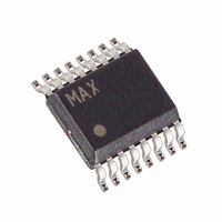
MAX1113CEE+ Maxim Integrated Products, MAX1113CEE+ Datasheet - Page 5

MAX1113CEE+
Manufacturer Part Number
MAX1113CEE+
Description
IC ADC 8-BIT 50KSPS 16-QSOP
Manufacturer
Maxim Integrated Products
Datasheet
1.MAX1113CEE.pdf
(20 pages)
Specifications of MAX1113CEE+
Number Of Bits
8
Sampling Rate (per Second)
50k
Data Interface
MICROWIRE™, QSPI™, Serial, SPI™
Number Of Converters
1
Power Dissipation (max)
680µW
Voltage Supply Source
Single Supply
Operating Temperature
0°C ~ 70°C
Mounting Type
Surface Mount
Package / Case
16-SSOP (0.150", 3.90mm Width)
Number Of Adc Inputs
4
Architecture
SAR
Conversion Rate
50 KSPs
Resolution
8 bit
Input Type
Differential
Interface Type
4-Wire (SPI, QSPI, MICROWIRE)
Voltage Reference
Internal 4.096 V or External
Supply Voltage (max)
5.5 V
Supply Voltage (min)
4.5 V
Maximum Power Dissipation
667 mW
Maximum Operating Temperature
+ 70 C
Mounting Style
SMD/SMT
Minimum Operating Temperature
0 C
Lead Free Status / RoHS Status
Lead free / RoHS Compliant
TIMING CHARACTERISTICS (Figures 8 and 9)
(V
Note 1:
Note 2: V
Note 3: On-channel grounded; sine wave applied to all off-channels.
Note 4: Conversion time is defined as the number of clock cycles multiplied by the clock period; clock has 50% duty cycle.
Note 5: Guaranteed by design. Not subject to production testing.
Note 6: Common-mode range for the analog inputs is from AGND to V
Note 7: External load should not change during the conversion for specified accuracy.
Note 8: External reference at 4.096V, full-scale input, 500kHz external clock.
Note 9: Measured as
Note 10: 1µF at REFOUT; internal reference settling to 0.5LSB.
Track/Hold Acquisition Time
DIN to SCLK Setup
DIN to SCLK Hold
SCLK Fall to Output Data Valid
CS Fall to Output Enable
CS Rise to Output Disable
CS to SCLK Rise Setup
CS to SCLK Rise Hold
SCLK Pulse Width High
SCLK Pulse Width Low
SCLK Fall to SSTRB
CS Fall to SSTRB Output Enable
(Note 5)
CS Rise to SSTRB Output
Disable (Note 5)
SSTRB Rise to SCLK Rise
(Note 5)
Wakeup Time
DD
= +4.5V to +5.5V, T
Relative accuracy is the analog value’s deviation (at any code) from its theoretical value after the full-scale range is calibrated.
PARAMETER
REFIN
= 4.096V, offset nulled.
_______________________________________________________________________________________
A
V
FS
= T
(4.5V) - V
MIN
to T
SYMBOL
MAX
FS
t
t
SSTRB
t
WAKE
t
t
t
t
t
ACQ
t
t
t
t
CSH
t
SCK
t
CSS
t
SDV
STR
DO
(5.5V)
DS
DH
DV
CH
TR
CL
, unless otherwise noted.)
+5V, Low-Power, Multi-Channel,
.
Figure 1,
C
Figure 1, C
Figure 2, C
C
Figure 1, external clock mode only,
C
Figure 2, external clock mode only,
C
Figure 11, internal clock mode only
External reference
Internal reference (Note 10)
LOAD
LOAD
LOAD
LOAD
= 100pF
= 100pF
= 100pF
= 100pF
LOAD
LOAD
CONDITIONS
= 100pF
= 100pF
DD
MAX111_C/E
MAX111_M
.
Serial 8-Bit ADCs
MIN
100
100
200
200
20
20
1
0
0
0
TYP
20
24
MAX
200
240
240
240
240
240
240
UNITS
ms
µs
ns
ns
ns
ns
ns
ns
ns
ns
ns
ns
ns
ns
ns
µs
5


