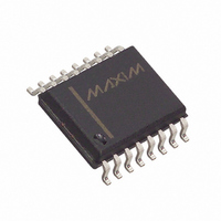
MAX110BCWE+ Maxim Integrated Products, MAX110BCWE+ Datasheet - Page 5

MAX110BCWE+
Manufacturer Part Number
MAX110BCWE+
Description
IC ADC SERIAL 2CH 14BIT 16-SOIC
Manufacturer
Maxim Integrated Products
Datasheet
1.MAX110BCPE.pdf
(24 pages)
Specifications of MAX110BCWE+
Number Of Bits
14
Sampling Rate (per Second)
50
Data Interface
MICROWIRE™, QSPI™, Serial, SPI™
Number Of Converters
1
Power Dissipation (max)
762mW
Voltage Supply Source
Single Supply
Operating Temperature
0°C ~ 70°C
Mounting Type
Surface Mount
Package / Case
16-SOIC (0.300", 7.50mm Width)
Number Of Adc Inputs
2
Architecture
Delta-Sigma
Conversion Rate
0.05 KSPs
Resolution
14 bit
Input Type
Differential
Interface Type
3-Wire (SPI, QSPI, MICROWIRE)
Voltage Reference
External
Supply Voltage (max)
5 V
Maximum Power Dissipation
762 mW
Maximum Operating Temperature
+ 70 C
Mounting Style
SMD/SMT
Minimum Operating Temperature
0 C
Lead Free Status / RoHS Status
Lead free / RoHS Compliant
ELECTRICAL CHARACTERISTICS—MAX111 (continued)
(V
unless otherwise noted. Typical values are at T
REFERENCE INPUTS
Differential Reference
Input Voltage Range
Absolute Reference Input
Voltage Range
Reference Input Current
Reference Input
Capacitance
Synchronous Conversion
Time (Note 7)
Oversampling Clock
Frequency
Input High Voltage
Input Low Voltage
Input Capacitance
Input Leakage Current
Output Low Voltage
Output High Voltage
Leakage Current
Output Capacitance
Positive Supply Voltage
Supply Current
Power-Down Current
CONVERSION TIME
DIGITAL INPUTS (CS, SCLK, DIN, and XCLK when RCSEL = 0V)
DIGITAL OUTPUTS (DOUT, BUSY, and XCLK when RCSEL = V
POWER REQUIREMENTS (all digital inputs at 0V or 5V)
DD
= 5V ±5%, f
PARAMETER
XCLK
Low-Cost, 2-Channel, ±14-Bit Serial ADCs
_______________________________________________________________________________________
= 1MHz, ÷ 2 mode (DV2 = 1), 81,920 CLK cycles/conv, V
SYMBOL
V
I
t
V
V
REF+
I
CONV
f
I
I
REF+
V
V
V
REF-
OSC
I
I
V
LKG
LKG
REF-
V
REF
DD
DD
OH
DD
OL
IH
IL
,
,
V
(Note 3)
10,240 clock-cycles/conversion
102,400 clock-cycles/conversion
(Note 8)
(Note 3)
Digital inputs at 0V or 5V
DOUT, BUSY, I
XCLK, I
DOUT, BUSY, V
XCLK, V
V
(Note 3)
Performance guaranteed by supply rejection test
V
V
REF+
OUT
DD
DD
= 5.25V
= 5.25V, V
A
= 5V or 0V
= 1.5V, V
= +25°C.)
SINK
DD
= 4.75V, I
= 200µA
SINK
XCLK
DD
REF-
= 4.75V, I
= 1.6mA
CONDITIONS
= 0V
= 0V, PD = 1
SOURCE
f
continuous-conversion mode
XCLK unloaded,
continuous-conversion mode, RC
oscillator operational (Note 9)
XCLK
DD
)
= 500kHz,
SOURCE
= 200µA
= 1.0mA
REF+
= 1.5V, V
REF-
V
V
= 0V, T
DD
DD
0.25
4.75
MIN
2.4
0
0
- 0.5
- 0.5
A
204.80
20.48
= T
TYP
640
960
4
MIN
V
to T
DD
MAX
1200
1.25
5.25
500
1.5
0.8
0.4
0.4
±1
±1
10
10
10
10
MAX
- 3.2
,
UNITS
MHz
ms
nA
pF
pF
µA
µA
pF
µA
µA
V
V
V
V
V
V
V
5


