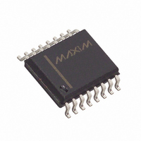
MAX110BCWE+ Maxim Integrated Products, MAX110BCWE+ Datasheet - Page 6

MAX110BCWE+
Manufacturer Part Number
MAX110BCWE+
Description
IC ADC SERIAL 2CH 14BIT 16-SOIC
Manufacturer
Maxim Integrated Products
Datasheet
1.MAX110BCPE.pdf
(24 pages)
Specifications of MAX110BCWE+
Number Of Bits
14
Sampling Rate (per Second)
50
Data Interface
MICROWIRE™, QSPI™, Serial, SPI™
Number Of Converters
1
Power Dissipation (max)
762mW
Voltage Supply Source
Single Supply
Operating Temperature
0°C ~ 70°C
Mounting Type
Surface Mount
Package / Case
16-SOIC (0.300", 7.50mm Width)
Number Of Adc Inputs
2
Architecture
Delta-Sigma
Conversion Rate
0.05 KSPs
Resolution
14 bit
Input Type
Differential
Interface Type
3-Wire (SPI, QSPI, MICROWIRE)
Voltage Reference
External
Supply Voltage (max)
5 V
Maximum Power Dissipation
762 mW
Maximum Operating Temperature
+ 70 C
Mounting Style
SMD/SMT
Minimum Operating Temperature
0 C
Lead Free Status / RoHS Status
Lead free / RoHS Compliant
Low-Cost, 2-Channel, ±14-Bit Serial ADCs
TIMING CHARACTERISTICS (see Figure 6)
(V
6
Note 1: These specifications apply after auto-null and gain calibration. Performance at power-supply tolerance limits is guaranteed
Note 2: 32,768 LSBs cover an input voltage range of ±V
Note 3: Guaranteed by design. Not subject to production testing.
Note 4: DNL is less than ±2 counts (LSBs) out of 2
Note 5: See 3-Step Calibration section in text.
Note 6: V
Note 7: Conversion time is set by control bits CONV1–CONV4.
Note 8: Tested at clock frequency of 1MHz with the divide-by-2 mode (i.e. oversampling clock of 500kHz). See Typical Operating
Note 9: This current depends strongly on C
Note 10: Timing specifications are guaranteed by design. All input control signals are specified with t
CS to SCLK Setup Time
(Note 10)
CS to SCLK Hold Time
(Note 10)
DIN to SCLK Setup Time
(Note 10)
DIN to SCLK Hold Time
(Note 10)
SCLK, XCLK Pulse Width
(Note 10)
Data Access Time
(Note 10)
SCLK to DOUT Valid
Delay (Note 10)
Bus Relinquish Time
(Note 10)
RC Oscillator Frequency
DD
_______________________________________________________________________________________
= 5V, V
PARAMETER
by power-supply rejection tests. Tests are performed at V
improved by averaging.
the negative input terminal exceeds the voltage at the positive input terminal.
Characteristics section for the effect of other clock frequencies. Also read the Clock Frequency section.
(10% to 90% of +5V) and timed from a +1.6V voltage level.
REF
SS
= (V
= -5V (MAX110), T
REF+
- V
REF-
SYMBOL
), V
t
t
t
t
t
CSS
CSH
t
t
t
DH
DO
DH
DS
CK
DA
A
IN
= T
= (V
MIN
T
MAX11_ _C/E
MAX11_ BM
T
MAX11_ _C/E
MAX11_ BM
T
MAX11_ _C/E
MAX11_ BM
C
C
T
MAX11_ _C/E/M
T
MAX11_ _C/E
MAX11_ BM
IN1+
A
A
A
A
A
LOAD
LOAD
to T
= +25°C
= +25°C
= +25°C
= +25°C
= +25°C
XCLK
- V
MAX
= 50pF
= 50pF
IN1-
(see Applications Information section).
, unless otherwise noted. Typical values are at T
15
) or (V
counts (±14 bits). The major source of DNL is noise, and this can be further
REF
IN2+
(15 bits). An additional bit (OFL) is set for V
CONDITIONS
- V
IN2-
DD
= 5V and V
). The voltage is interpreted as negative when the voltage at
T
MAX11_ _C/E
MAX11_ BM
T
MAX11_ _C/E
MAX11_ BM
A
A
= +25°C
= +25°C
SS
= -5V (MAX110).
A
MIN
100
100
100
120
160
= +25°C.)
1.3
1.1
60
80
60
80
0
0
0
0
0
0
0
0
r
= t
IN
f
> V
= 5ns
TYP
2.0
35
60
35
REF
.
MAX
100
120
100
120
140
120
2.8
3.0
80
80
UNITS
MHz
ns
ns
ns
ns
ns
ns
ns
ns


