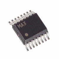
MAX1247BCEE+ Maxim Integrated Products, MAX1247BCEE+ Datasheet - Page 12

MAX1247BCEE+
Manufacturer Part Number
MAX1247BCEE+
Description
IC ADC SRL 4CH 12BIT 2.7V 16QSOP
Manufacturer
Maxim Integrated Products
Datasheet
1.MAX1247BCEE.pdf
(25 pages)
Specifications of MAX1247BCEE+
Number Of Bits
12
Sampling Rate (per Second)
133k
Data Interface
MICROWIRE™, QSPI™, Serial, SPI™
Number Of Converters
1
Power Dissipation (max)
667mW
Voltage Supply Source
Single Supply
Operating Temperature
0°C ~ 70°C
Mounting Type
Surface Mount
Package / Case
16-SSOP (0.150", 3.90mm Width)
Number Of Adc Inputs
4
Architecture
SAR
Conversion Rate
133 KSPs
Resolution
12 bit
Interface Type
4-Wire (SPI, QSPI, MICROWIRE, TMS320)
Voltage Reference
External
Supply Voltage (max)
5 V
Supply Voltage (min)
3 V
Mounting Style
SMD/SMT
Lead Free Status / RoHS Status
Lead free / RoHS Compliant
+2.7V, Low-Power, 4-Channel,
Serial 12-Bit ADCs in QSOP-16
Table 2. Channel Selection in Single-Ended Mode (SGL/D D I I F F = 1)
Table 3. Channel Selection in Differential Mode (SGL/D D I I F F = 0)
Circuit, the simplest software interface requires only
three 8-bit transfers to perform a conversion (one 8-bit
transfer to configure the ADC, and two more 8-bit trans-
fers to clock out the 12-bit conversion result). See Figure
19 for MAX1246/MAX1247 QSPI connections.
Make sure the CPU’s serial interface runs in master
mode so the CPU generates the serial clock. Choose a
clock frequency from 100kHz to 2MHz.
Figure 5 shows the timing for this sequence. Bytes RB2
and RB3 contain the result of the conversion, padded
with one leading zero and three trailing zeros. The total
conversion time is a function of the serial-clock fre-
quency and the amount of idle time between 8-bit
transfers. To avoid excessive T/H droop, make sure the
total conversion time does not exceed 120µs.
12
1) Set up the control byte for external clock mode and
2) Use a general-purpose I/O line on the CPU to pull
3) Transmit TB1 and, simultaneously, receive a byte
4) Transmit a byte of all zeros ($00 hex) and, simulta-
5) Transmit a byte of all zeros ($00 hex) and, simulta-
6) Pull CS high.
SEL2
SEL2
call it TB1. TB1 should be of the format: 1XXXXX11
binary, where the Xs denote the particular channel
and conversion mode selected.
CS low.
and call it RB1. Ignore RB1.
neously, receive byte RB2.
neously, receive byte RB3.
______________________________________________________________________________________
0
1
0
1
0
0
1
1
SEL1
0
0
1
1
SEL1
0
1
0
1
Simple Software Interface
SEL0
1
1
0
0
SEL0
1
0
1
0
CH0
+
CH0
+
–
In unipolar input mode, the output is straight binary
(Figure 16). For bipolar inputs, the output is two’s com-
plement (Figure 17). Data is clocked out at the falling
edge of SCLK in MSB-first format.
The MAX1246/MAX1247 may use either an external
serial clock or the internal clock to perform the succes-
sive-approximation conversion. In both clock modes,
the external clock shifts data in and out of the
MAX1246/MAX1247. The T/H acquires the input signal
as the last three bits of the control byte are clocked into
DIN. Bits PD1 and PD0 of the control byte program the
clock mode. Figures 6–9 show the timing characteristics
common to both modes.
In external clock mode, the external clock not only shifts
data in and out, but it also drives the analog-to-digital
conversion steps. SSTRB pulses high for one clock
period after the last bit of the control byte. Succes-
sive-approximation bit decisions are made and appear
at DOUT on each of the next 12 SCLK falling edges
(Figure 5). SSTRB and DOUT go into a high-impedance
state when CS goes high; after the next CS falling edge,
SSTRB outputs a logic low. Figure 7 shows the SSTRB
timing in external clock mode.
The conversion must complete in some minimum time,
or droop on the sample-and-hold capacitors may
degrade conversion results. Use internal clock mode if
the serial clock frequency is less than 100kHz, or if
serial clock interruptions could cause the conversion
interval to exceed 120µs.
CH1
+
CH1
+
–
CH2
+
CH2
+
–
CH3
+
Clock Modes
External Clock
Digital Output
CH3
COM
+
–
–
–
–
–


