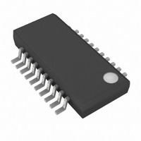
MAX1228BEEP+ Maxim Integrated Products, MAX1228BEEP+ Datasheet - Page 8

MAX1228BEEP+
Manufacturer Part Number
MAX1228BEEP+
Description
IC ADC 12BIT 300KSPS 20-QSOP
Manufacturer
Maxim Integrated Products
Datasheet
1.MAX1228BEEP.pdf
(23 pages)
Specifications of MAX1228BEEP+
Number Of Bits
12
Sampling Rate (per Second)
300k
Data Interface
MICROWIRE™, QSPI™, Serial, SPI™
Number Of Converters
1
Power Dissipation (max)
727mW
Voltage Supply Source
Single Supply
Operating Temperature
-40°C ~ 85°C
Mounting Type
Surface Mount
Package / Case
20-QSOP
Number Of Adc Inputs
12
Architecture
SAR
Conversion Rate
300 KSPs
Resolution
12 bit
Interface Type
Serial
Voltage Reference
Internal 4.096 V or External
Supply Voltage (max)
5 V
Mounting Style
SMD/SMT
Lead Free Status / RoHS Status
Lead free / RoHS Compliant
12-Bit 300ksps ADCs with FIFO,
Temp Sensor, Internal Reference
8
MAX1230
2–12, 26,
19, 25
27, 28
TQFN
1, 17,
_______________________________________________________________________________________
13
14
15
16
18
20
21
22
23
24
—
—
—
—
—
—
—
MAX1230
QSOP
1–14
15
16
17
18
19
20
21
22
23
24
—
—
—
—
—
—
—
—
MAX1228
1–10
11
12
13
14
15
16
17
18
19
20
—
—
—
—
—
—
—
—
MAX1226
1–6
10
11
12
13
14
15
16
—
—
—
—
—
—
—
—
7
8
9
REF-/AIN14
REF-/AIN10
REF-/AIN6
AIN0–13
CNVST/
CNVST/
CNVST/
AIN0–9
AIN0–5
NAME
AIN15
AIN11
DOUT
REF+
SCLK
AIN7
GND
EOC
N.C.
V
DIN
CS
EP
DD
No Connection. Not internally connected.
Analog Inputs
Analog Inputs
Analog Inputs
Negative Input for External Differential Reference/Analog Input 14.
See Table 3 for details on programming the setup register.
Negative Input for External Differential Reference/Analog Input 10.
See Table 3 for details on programming the setup register.
Negative Input for External Differential Reference/Analog Input 6.
See Table 3 for details on programming the setup register.
Active-Low Conversion Start Input/Analog Input 15. See Table 3
for details on programming the setup register.
Active-Low Conversion Start Input/Analog Input 11. See Table 3
for details on programming the setup register.
Active-Low Conversion Start Input/Analog Input 7. See Table 3 for
details on programming the setup register.
Positive Reference Input. Bypass to GND with a 0.1µF capacitor.
Ground
Power Input. Bypass to GND with a 0.1µF capacitor.
Serial Clock Input. Clocks data in and out of the serial interface.
(Duty cycle must be 40% to 60%.) See Table 3 for details on
programming the clock mode.
Active-Low Chip-Select Input. When CS is low, the serial interface
is enabled. When CS is high, DOUT is high impedance.
Serial Data Input. DIN data is latched into the serial interface on
the rising edge of SCLK.
Serial Data Output. Data is clocked out on the falling edge of
SCLK. High impedance when CS is connected to V
End of Conversion Output. Data is valid after EOC pulls low.
Exposed Pad. Internally connected to GND. Connect to a large
ground plane to maximize thermal performance. Not intended as
an electrical connection point.
FUNCTION
Pin Description
DD
.


