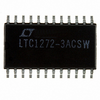
LTC1272-3ACSW Linear Technology, LTC1272-3ACSW Datasheet - Page 13

LTC1272-3ACSW
Manufacturer Part Number
LTC1272-3ACSW
Description
IC A/D CONV 12BIT SAMPLNG 24SOIC
Manufacturer
Linear Technology
Datasheet
1.LTC1272-3CCSW.pdf
(20 pages)
Specifications of LTC1272-3ACSW
Number Of Bits
12
Sampling Rate (per Second)
250k
Data Interface
Parallel
Number Of Converters
1
Power Dissipation (max)
75mW
Voltage Supply Source
Single Supply
Operating Temperature
0°C ~ 70°C
Mounting Type
Surface Mount
Package / Case
24-SOIC (0.300", 7.50mm Width)
Lead Free Status / RoHS Status
Contains lead / RoHS non-compliant
Available stocks
Company
Part Number
Manufacturer
Quantity
Price
Company:
Part Number:
LTC1272-3ACSW
Manufacturer:
ISSI
Quantity:
448
Part Number:
LTC1272-3ACSW
Manufacturer:
LINEAR/凌特
Quantity:
20 000
A
Table 2. Slow Memory Mode, Parallel Read Data Bus Status
Data Outputs
Read
Data Format
The output data format can be either a complete parallel
load for 16-bit microprocessors or a two byte load for
8-bit microprocessors. Data is always right justified (i.e.,
LSB is the most right-hand bit in a 16-bit word). For a two
byte read, only data outputs D7. . . D0/8 are used. Byte
selection is governed by the HBEN input which controls an
internal digital multiplexer. This multiplexes the 12 bits of
conversion data onto the lower D7. . . D0/8 outputs
(4MSBs or 8LSBs) where it can be read in two read cycles.
The 4MSBs always appear on D11 . . . D8 whenever the
three-state output drives are turned on.
Slow Memory Mode, Parallel Read (HBEN = Low)
Figure 14 and Table 2 show the timing diagram and data
bus status for Slow Memory Mode, Parallel Read. CS and
RD going low triggers a conversion and the LTC1272
acknowledges by taking BUSY low. Data from the previous
conversion appears on the three-state data outputs. BUSY
returns high at the end of conversion when the output
latches have been updated and the conversion result is
placed on data outputs D11 . . . D0/8.
PPLICATI
DB11
D11
O
U
S
DB10
D10
TRACK
I FOR ATIO
BUSY
HOLD
DATA
U
RD
RD
CS
Figure 14. Slow Memory Mode, Parallel Read Timing Diagram
DB9
D9
t
1
W
t
t
12
t
3
2
DB8
D8
OLD DATA
DB11-DB0
t
CONV
U
DB7
D7
t
6
DB6
D6
Slow Memory Mode, Two Byte Read
For a two byte read, only 8 data outputs D7 . . . D0/8 are
used. Conversion start procedure and data output status
for the first read operation is identical to Slow Memory
Mode, Parallel Read. See Figure 15 timing diagram and
Table 3 data bus status. At the end of conversion the low
data byte (DB7 . . . DB0) is read from the ADC. A second
Read operation with HBEN high, places the high byte on
data outputs D3/11 . . . D0/8 and disables conversion start.
Note the 4MSBs appear on data outputs D11 . . . D8 during
the two Read operations above.
ROM Mode, Parallel Read (HBEN = Low)
The ROM Mode avoids placing a microprocessor into a
Wait state. A conversion is started with a Read operation
and the 12 bits of data from the previous conversion is
available on data outputs D11 . . . D0/8 (see Figure 16 and
Table 4). This data may be disregarded if not required. A
second Read operation reads the new data (DB11 . . . DB0)
and starts another conversion. A delay at least as long as
the LTC1272 conversion time plus the 1µs minimum delay
between conversions must be allowed between Read
operations.
NEW DATA
DB11-DB0
DB5
D5
t
t
7
5
t
11
DB4
D4
t
10
D3/11
DB3
t
1
LTC1272 • TA16
D2/10
DB2
LTC1272
D1/9
DB1
13
D0/8
DB0
1272fb


