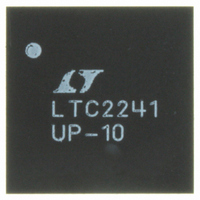
LTC2241CUP-10#PBF Linear Technology, LTC2241CUP-10#PBF Datasheet - Page 19

LTC2241CUP-10#PBF
Manufacturer Part Number
LTC2241CUP-10#PBF
Description
IC ADC 10BIT 210MSPS 64-QFN
Manufacturer
Linear Technology
Datasheet
1.LTC2241CUP-10PBF.pdf
(28 pages)
Specifications of LTC2241CUP-10#PBF
Number Of Bits
10
Sampling Rate (per Second)
210M
Data Interface
Parallel
Number Of Converters
1
Power Dissipation (max)
805mW
Voltage Supply Source
Single Supply
Operating Temperature
0°C ~ 70°C
Mounting Type
Surface Mount
Package / Case
64-WFQFN, Exposed Pad
Lead Free Status / RoHS Status
Lead free / RoHS Compliant
Available stocks
Company
Part Number
Manufacturer
Quantity
Price
APPLICATIONS INFORMATION
Maximum and Minimum Encode Rates
The maximum encode rate for the LTC2241-10 is 210Msps.
For the ADC to operate properly, the encode signal should
have a 50% (±5%) duty cycle. Each half cycle must have at
least 2.26ns for the ADC internal circuitry to have enough
settling time for proper operation. Achieving a precise 50%
duty cycle is easy with differential sinusoidal drive using
a transformer or using symmetric differential logic such
as PECL or LVDS.
An optional clock duty cycle stabilizer circuit can be used if
the input clock has a non 50% duty cycle. This circuit uses
the rising edge of the ENC
The falling edge of ENC
edge is generated by a phase-locked loop. The input clock
duty cycle can vary from 40% to 60% and the clock duty
cycle stabilizer will maintain a constant 50% internal duty
V
THRESHOLD
Figure 12a. Single-Ended ENC Drive,
Not Recommended for Low Jitter
= 1.5V
CLOCK
INPUT
0.1μF
+
is ignored and the internal falling
+
pin to sample the analog input.
1.5V
0.1μF
0.1μF
ENC
ENC
•
ETC1-1-13
MA/COM
+
–
T1
LTC2241-10
•
224110 F12a
50Ω
50Ω
Figure 11. Transformer Driven ENC
0.1μF
8.2pF
100Ω
ENC –
ENC
+
LTC2241-10
V
V
cycle. If the clock is turned off for a long period of time,
the duty cycle stabilizer circuit will require one hundred
clock cycles for the PLL to lock onto the input clock. To
use the clock duty cycle stabilizer, the MODE pin should be
connected to 1/3V
The lower limit of the LTC2241-10 sample rate is determined
by droop of the sample-and-hold circuits. The pipelined
architecture of this ADC relies on storing analog signals on
small valued capacitors. Junction leakage will discharge
the capacitors. The specifi ed minimum operating frequency
for the LTC2241-10 is 1Msps.
DIGITAL OUTPUTS
Table 1 shows the relationship between the analog input
voltage, the digital data bits, and the overfl ow bit.
DD
DD
1.5V BIAS
1.5V BIAS
4.8k
4.8k
+
/ENC
CLOCK
V
Figure 12b. ENC Drive Using LVDS
DD
LVDS
–
DD
100Ω
or 2/3V
ADC CIRCUITS
TO INTERNAL
0.1μF
0.1μF
DD
ENC
ENC
224110 F11
using external resistors.
+
–
LTC2241-10
LTC2241-10
224110 F12b
19
224110fb


