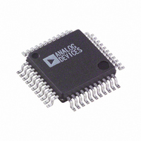
AD7859LASZ Analog Devices Inc, AD7859LASZ Datasheet - Page 7

AD7859LASZ
Manufacturer Part Number
AD7859LASZ
Description
IC ADC 12BIT 8CH 200KSPS 44-MQFP
Manufacturer
Analog Devices Inc
Datasheet
1.AD7859LASZ.pdf
(28 pages)
Specifications of AD7859LASZ
Data Interface
Parallel
Number Of Bits
12
Sampling Rate (per Second)
100k
Number Of Converters
2
Power Dissipation (max)
30mW
Voltage Supply Source
Analog and Digital
Operating Temperature
-40°C ~ 85°C
Mounting Type
Surface Mount
Package / Case
44-MQFP, 44-PQFP
Resolution (bits)
12bit
Sampling Rate
100kSPS
Input Channel Type
Single Ended
Supply Current
1.95mA
Digital Ic Case Style
QFP
No. Of Pins
44
Lead Free Status / RoHS Status
Lead free / RoHS Compliant
Available stocks
Company
Part Number
Manufacturer
Quantity
Price
Company:
Part Number:
AD7859LASZ
Manufacturer:
Analog Devices Inc
Quantity:
10 000
Part Number:
AD7859LASZ
Manufacturer:
ADI/亚德诺
Quantity:
20 000
Company:
Part Number:
AD7859LASZ-REEL
Manufacturer:
Analog Devices Inc
Quantity:
10 000
REV. A
Mnemonic
CONVST
RD
WR
CS
REF
REF
AV
AGND
DV
DGND
C
C
AIN1–AIN8
W/B
DB0–DB7
DB8/HBEN
DB9–DB15
CLKIN
CAL
BUSY
SLEEP
NC
REF1
REF2
DD
DD
IN
OUT
/
Analog Ground. Ground reference for track/hold, reference and DAC.
Digital Ground. Ground reference point for digital circuitry.
Analog Inputs. Eight analog inputs which can be used as eight single ended inputs (referenced to AGND) or four
Data Bits 0 to 7. Three state data I/O pins that are controlled by CS, RD and WR. Data output is straight binary
Data Bit 8/High Byte Enable. When W/B is high, this pin acts as Data Bit 7, a three state data I/O pin that is con-
Data Bits 9 to 15. Three state data I/O pins that are controlled by CS, RD and WR. Data output is straight bi-
Master Clock Signal for the device (4 MHz for AD7859, 1.8 MHz for AD7859L). Sets the conversion and calibra-
Busy Output. The busy output is triggered high when a conversion or a calibration is initiated, and remains high
Description
Convert Start. Logic input. A low to high transition on this input puts the track/hold into its hold
mode and starts conversion. When this input is not used, it should be tied to DV
Read Input. Active low logic input. Used in conjunction with CS to read from internal registers.
Write Input. Active low logic input. Used in conjunction with CS to write to internal registers.
Chip Select Input. Active low logic input. The device is selected when this input is active.
Reference Input/Output. This pin is connected to the internal reference through a series resistor and is the
reference source for the analog-to-digital converter. The nominal reference voltage is 2.5 V and this appears at the
pin. This pin can be overdriven by an external reference or can be taken as high as AV
AV
Analog Supply Voltage, +3.0 V to +5.5 V.
Digital Supply Voltage, +3.0 V to +5.5 V.
Reference Capacitor (0.1 F multilayer ceramic). This external capacitor is used as a charge source for the inter-
nal DAC. The capacitor should be tied between the pin and AGND.
Reference Capacitor (0.01 F ceramic disc). This external capacitor is used in conjunction with the on-chip refer-
ence. The capacitor should be tied between the pin and AGND.
pseudo differential inputs. Channel configuration is selected by writing to the control register. None of the inputs
can go below AGND or above AV
Word/Byte input. When this input is at a logic 1, data is transferred to and from the AD7859/AD7859L in 16-bit
words on pins DB0 to DB15. When this pin is at a Logic 0, byte transfer mode is enabled. Data is transferred on
pins DB0 to DB7 and pin DB8/HBEN assumes its HBEN functionality.
(unipolar mode) or twos complement (bipolar mode).
trolled by CS, RD and WR. When W/B is low, this pin acts as the High Byte Enable pin. When HBEN is low,
then the low byte of data being written to or read from the AD7859/AD7859L is on DB0 to DB7. When HBEN
is high, then the high byte of data being written to or read from the AD7859/AD7859L is on DB0 to DB7.
nary (unipolar mode) or twos complement (bipolar mode).
tion times.
Calibration Input. A logic 0 in this pin resets all logic. A rising edge on this pin initiates a calibration. This input
overrides all other internal operations.
until the conversion or calibration is completed.
Sleep Input. This pin is used in conjunction with the PGMT0 and PGMT1 bits in the control register to deter-
mine the power-down mode. Please see the “Power-Down Options” section for details.
No connect pins. These pins should be left unconnected.
DD
, then the C
REF1
pin should also be tied to AV
PIN FUNCTION DESCRIPTION
DD
at any time. See Table III for channel selection.
–7–
DD
.
DD
AD7859/AD7859L
.
DD
. When this pin is tied to


