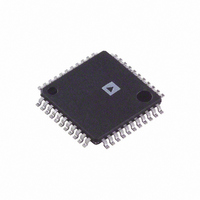
AD9042ASTZ Analog Devices Inc, AD9042ASTZ Datasheet - Page 6

AD9042ASTZ
Manufacturer Part Number
AD9042ASTZ
Description
IC ADC 12BIT 41MSPS 44-TQFP
Manufacturer
Analog Devices Inc
Datasheet
1.AD9042ASTZ.pdf
(24 pages)
Specifications of AD9042ASTZ
Data Interface
Parallel
Number Of Bits
12
Sampling Rate (per Second)
41M
Number Of Converters
3
Power Dissipation (max)
735mW
Voltage Supply Source
Analog and Digital, Dual ±
Operating Temperature
-40°C ~ 85°C
Mounting Type
Surface Mount
Package / Case
44-TQFP, 44-VQFP
Resolution (bits)
12bit
Sampling Rate
41MSPS
Input Channel Type
Single Ended
Supply Voltage Range - Analog
5V
Supply Voltage Range - Digital
5V
Supply Current
119mA
Number Of Elements
1
Resolution
12Bit
Architecture
Pipelined
Sample Rate
41MSPS
Input Polarity
Unipolar
Input Type
Voltage
Rated Input Volt
1.9/2.9V
Differential Input
No
Power Supply Requirement
Single
Single Supply Voltage (typ)
5V
Single Supply Voltage (min)
4.75V
Single Supply Voltage (max)
5.25V
Dual Supply Voltage (typ)
Not RequiredV
Dual Supply Voltage (min)
Not RequiredV
Dual Supply Voltage (max)
Not RequiredV
Power Dissipation
735mW
Differential Linearity Error
±1LSB
Integral Nonlinearity Error
±0.75LSB(Typ)
Operating Temp Range
-40C to 85C
Operating Temperature Classification
Industrial
Mounting
Surface Mount
Pin Count
44
Package Type
LQFP
Input Signal Type
Single-Ended
Lead Free Status / RoHS Status
Lead free / RoHS Compliant
Lead Free Status / RoHS Status
Lead free / RoHS Compliant, Lead free / RoHS Compliant
Available stocks
Company
Part Number
Manufacturer
Quantity
Price
Company:
Part Number:
AD9042ASTZ
Manufacturer:
Analog Devices Inc
Quantity:
10 000
Part Number:
AD9042ASTZ
Manufacturer:
ADI/亚德诺
Quantity:
20 000
AD9042
ABSOLUTE MAXIMUM RATINGS
Table 4.
Parameter
AV
DV
Analog Input Voltage
Analog Input Current
Digital Input Voltage (ENCODE)
ENCODE, ENCODE Differential Voltage
Digital Output Current
Operating Temperature Range (Ambient)
Maximum Junction Temperature
Lead Temperature (Soldering, 10 sec)
Storage Temperature Range (Ambient)
1
Absolute maximum ratings are limiting values to be applied individually, and
beyond which the serviceability of the circuit may be impaired.
CC
CC
Voltage
Voltage
1
Rating
0 V to 7 V
0 V to 7 V
0.5 V to 4.5 V
20 mA
0 V to AV
4 V
−40 to +40 mA
−40 °C to +85°C
+150°C
+300°C
−65°C to +150°C
CC
Rev. B | Page 6 of 24
III.
IV.
VI.
II.
V.
I.
Stresses above those listed under Absolute Maximum Ratings
may cause permanent damage to the device. This is a stress
rating only; functional operation of the device at these or any
other conditions above those indicated in the operational
section of this specification is not implied. Exposure to absolute
maximum rating conditions for extended periods may affect
device reliability.
THERMAL RESISTANCE
θ
soldered in a circuit board for surface-mount packages.
Table 5. Thermal Resistance
Package Type
44-Lead LQFP
EXPLANATION OF TEST LEVELS
ESD CAUTION
JA
is specified for the worst-case conditions, that is, a device
100% production tested.
100% production tested at +25°C, and sample tested at
specified temperatures. AC testing done on sample basis.
Sample tested only.
Parameter is guaranteed by design and characterization
testing.
Parameter is a typical value only.
100% production tested at +25°C; sample tested at
temperature extremes.
θ
55
JA
Unit
°C/W


