MAX1191ETI+ Maxim Integrated Products, MAX1191ETI+ Datasheet - Page 2

MAX1191ETI+
Manufacturer Part Number
MAX1191ETI+
Description
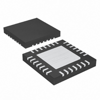
IC ADC 8BIT 7.5MSPS DUAL 28-TQFN
Manufacturer
Maxim Integrated Products
Datasheet
1.MAX1191ETI.pdf
(27 pages)
Specifications of MAX1191ETI+
Number Of Bits
8
Sampling Rate (per Second)
7.5M
Data Interface
Parallel
Number Of Converters
2
Voltage Supply Source
Single Supply
Operating Temperature
-40°C ~ 85°C
Mounting Type
Surface Mount
Package / Case
28-WFQFN Exposed Pad
Lead Free Status / RoHS Status
Lead free / RoHS Compliant
ABSOLUTE MAXIMUM RATINGS
V
OGND to GND.......................................................-0.3V to +0.3V
INA+, INA-, INB+, INB- to GND .................-0.3V to (V
CLK, REFIN, REFP, REFN, COM to GND ...-0.3V to (V
PD0, PD1 to OGND .................................-0.3V to (OV
Digital Outputs to OGND .........................-0.3V to (OV
Continuous Power Dissipation (T
Ultra-Low-Power, 7.5Msps, Dual 8-Bit ADC
Stresses beyond those listed under “Absolute Maximum Ratings” may cause permanent damage to the device. These are stress ratings only, and functional
operation of the device at these or any other conditions beyond those indicated in the operational sections of the specifications is not implied. Exposure to
absolute maximum rating conditions for extended periods may affect device reliability.
ELECTRICAL CHARACTERISTICS
(V
= 0.33µF, T
2
DD
DC ACCURACY
Resolution
Integral Nonlinearity
Differential Nonlinearity
Offset Error
Gain Error
DC Gain Matching
Gain Temperature Coefficient
Power-Supply Rejection
ANALOG INPUT
Differential Input Voltage Range
Common-Mode Input Voltage
Range
Input Resistance
Input Capacitance
CONVERSION RATE
Maximum Clock Frequency
Data Latency
DYNAMIC CHARACTERISTICS (differential inputs, 4096 point FFT)
Signal-to-Noise Ratio
(Note 2)
Signal-to-Noise and Distortion
(Note 2)
DD
28-Pin Thin QFN (derated 20.8mW/°C above +70°C) ...1667mW
, OV
_______________________________________________________________________________________
= 3.0V, OV
DD
A
PARAMETER
to GND ...............................................-0.3V to +3.6V
= -40°C to +85°C, unless otherwise noted. Typical values are at T
DD
= 1.8V, V
REFIN
A
= +70°C)
= V
SYMBOL
SINAD
V
V
DNL
SNR
f
DD
INL
R
C
COM
CLK
DIFF
IN
IN
(internal reference), C
No missing codes over temperature
≥+25°C
<+25°C
Excludes REFP - REFN error
Offset (V
Gain (V
Differential or single-ended inputs
Switched capacitor load
Channel A
Channel B
f
f
f
f
IN
IN
IN
IN
= 1.875MHz
= 3.75MHz
= 1.875MHz
= 3.75
DD
DD
DD
DD
DD
+ 0.3V)
+ 0.3V)
+ 0.3V)
+ 0.3V)
DD
±5%)
±5%)
CONDITIONS
L
≈ 10pF at digital outputs, f
Operating Temperature Range ...........................-40°C to +85°C
Junction Temperature ......................................................+150°C
Storage Temperature Range .............................-65°C to +150°C
Lead Temperature (soldering, 10s) .................................+300°C
A
= +25°C.) (Note 1)
CLK
MIN
7.5
47
47
8
= 7.5MHz, C
V
±0.512
±0.15
±0.13
±0.01
±0.05
TYP
±0.2
DD
48.7
48.6
48.6
48.5
±30
720
5.0
5.5
5
/ 2
REFP
= C
±1.00
±1.00
MAX
±0.2
±2
±4
±6
REFN
= C
ppm/°C
UNITS
cycles
Clock
%FS
%FS
MHz
LSB
LSB
LSB
Bits
dB
dB
dB
kΩ
pF
V
V
COM


