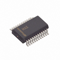
MAX1296BEEG+ Maxim Integrated Products, MAX1296BEEG+ Datasheet - Page 3

MAX1296BEEG+
Manufacturer Part Number
MAX1296BEEG+
Description
IC ADC 12BIT 420KSPS 24-QSOP
Manufacturer
Maxim Integrated Products
Datasheet
1.MAX1296BEEG.pdf
(19 pages)
Specifications of MAX1296BEEG+
Number Of Bits
12
Sampling Rate (per Second)
420k
Data Interface
Parallel
Number Of Converters
1
Power Dissipation (max)
762mW
Voltage Supply Source
Single Supply
Operating Temperature
-40°C ~ 85°C
Mounting Type
Surface Mount
Package / Case
24-QSOP
Number Of Adc Inputs
2
Architecture
SAR
Conversion Rate
420 KSPs
Resolution
12 bit
Voltage Reference
Internal 2.5 V or External
Supply Voltage (max)
5 V
Mounting Style
SMD/SMT
Lead Free Status / RoHS Status
Lead free / RoHS Compliant
ELECTRICAL CHARACTERISTICS (continued)
(V
T
A
ANALOG INPUTS
INTERNAL REFERENCE
EXTERNAL REFERENCE AT REF
DIGITAL INPUTS AND OUTPUTS
POWER REQUIREMENTS
Analog Input Voltage Range
Single-Ended and Differential
(Note 6)
Multiplexer Leakage Current
Input Capacitance
REF Output Voltage
REF Short-Circuit Current
REF Temperature Coefficient
REFADJ Input Range
REFADJ High Threshold
Load Regulation (Note 7)
Capacitive Bypass at REFADJ
Capacitive Bypass at REF
REF Input Voltage Range
REF Input Current
Input Voltage High
Input Voltage Low
Input Hysteresis
Input Leakage Current
Input Capacitance
Output Voltage Low
Output Voltage High
Three-State Leakage Current
Three-State Output Capacitance
Analog Supply Voltage
Positive Supply Current
Power-Supply Rejection
DD
= T
= +5V ±10%, COM = GND, REFADJ = V
MIN
PARAMETER
to T
with +2.5V Reference and Parallel Interface
MAX
, unless otherwise noted. Typical values are at T
_______________________________________________________________________________________
420ksps, +5V, 6-/2-Channel, 12-Bit ADCs
SYMBOL
I
LEAKAGE
TC
C
V
V
V
I
V
V
PSR
C
C
I
I
V
V
REF
V
I
REF
HYS
OUT
DD
DD
OH
IN
OL
DD
IN
REF
IH
IN
IL
IN
Unipolar, V
Bipolar, V
On/off-leakage current, V
For small adjustments
To power down the internal reference
0 to 0.5mA output load
V
Shutdown mode
V
I
I
CS = V
CS = V
Operating mode,
f
Standby mode
Shutdown mode
V
SINK
SOURCE
SAMPLE
REF
IN
DD
DD
= 0 or V
, V
= 5V ±10%, full-scale input
= 2.5V, f
= 1.6mA
DD
DD
REF
= 420ksps
= 1mA
COM
COM
= +2.5V, 4.7µF capacitor at REF pin, f
DD
SAMPLE
= V
CONDITIONS
= 0
REF
A
= +25°C.)
= 420ksps
/ 2
Internal reference
External reference
Internal reference
External reference
IN
= 0 or V
DD
V
-V
V
DD
DD
2.49
MIN
REF
4.7
1.0
4.0
4.5
0
CLK
- 0.5
- 1
/2
= 7.6MHz (50% duty cycle),
±0.01
±100
±0.1
±0.1
±0.3
TYP
0.01
±20
200
200
2.5
0.2
3.3
2.8
1.0
0.5
12
15
15
15
2
+V
V
50mV
MAX
V
±0.9
2.51
300
DD
REF
0.8
0.4
3.6
3.1
1.2
0.8
±1
±1
10
5.5
10
REF
±1
1
2
+
/2
ppm/°C
mV/mA
UNITS
mA
mV
mV
mA
mV
µA
pF
µF
µF
µA
µA
µA
pF
µA
pF
µA
V
V
V
V
V
V
V
V
V
3


