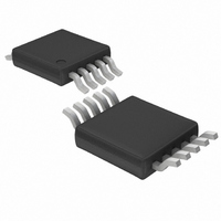
LTC2433-1IMS#TR Linear Technology, LTC2433-1IMS#TR Datasheet - Page 13

LTC2433-1IMS#TR
Manufacturer Part Number
LTC2433-1IMS#TR
Description
IC CONV A/D 16BIT DIFF 10-MSOP
Manufacturer
Linear Technology
Datasheet
1.LTC2433-1CMS.pdf
(28 pages)
Specifications of LTC2433-1IMS#TR
Number Of Bits
16
Sampling Rate (per Second)
6.8
Data Interface
MICROWIRE™, Serial, SPI™
Number Of Converters
2
Power Dissipation (max)
1mW
Voltage Supply Source
Single Supply
Operating Temperature
-40°C ~ 85°C
Mounting Type
Surface Mount
Package / Case
10-TFSOP, 10-MSOP (0.118", 3.00mm Width)
Lead Free Status / RoHS Status
Contains lead / RoHS non-compliant
Available stocks
Company
Part Number
Manufacturer
Quantity
Price
In addition, the CS signal can be used to trigger a new
conversion cycle before the entire serial data transfer has
been completed. The LTC2433-1 will abort any serial data
transfer in progress and start a new conversion cycle
anytime a LOW-to-HIGH transition is detected at the CS
pin after the converter has entered the data output state
(i.e., after the first rising edge of SCK occurs with
CS = LOW).
Finally, CS can be used to control the free-running modes
of operation, see Serial Interface Timing Modes section.
Grounding CS will force the ADC to continuously convert
at the maximum output rate selected by F
SERIAL INTERFACE TIMING MODES
The LTC2433-1’s 3-wire interface is SPI and MICROWIRE
compatible. This interface offers several flexible modes of
Table 4. LTC2433-1 Interface Timing Modes
Configuration
External SCK, Single Cycle Conversion
External SCK, 2-Wire I/O
Internal SCK, Single Cycle Conversion
Internal SCK, 2-Wire I/O, Continuous Conversion
APPLICATIO S I FOR ATIO
(EXTERNAL)
SDO
SCK
CS
Hi-Z
CONVERSION
TEST EOC
U
SLEEP
(OPTIONAL)
TEST EOC
U
SLEEP
Hi-Z
Figure 6. External Serial Clock, Single Cycle Operation
W
BIT 18
EOC
O
ANALOG INPUT RANGE
BIT 17
.
“O”
–0.5V
External
External
Internal
Internal
U
Source
REF
SCK
0.1V TO V
REFERENCE
TO 0.5V
VOLTAGE
BIT 16
SIG
1 F
2.7V TO 5.5V
REF
CC
BIT 15
MSB
1
2
3
4
5
6
V
REF
REF
IN
IN
GND
CC
LTC2433-1
+
–
+
–
operation. These include internal/external serial clock,
2- or 3-wire I/O, single cycle conversion and autostart. The
following sections describe each of these serial interface
timing modes in detail. In all these cases, the converter
can use the internal oscillator (F
oscillator connected to the F
summary.
External Serial Clock, Single Cycle Operation
(SPI/MICROWIRE Compatible)
This timing mode uses an external serial clock to shift out
the conversion result and a CS signal to monitor and
control the state of the conversion cycle, see Figure 6.
The serial clock mode is selected on the falling edge of CS.
To select the external serial clock mode, the serial clock pin
(SCK) must be LOW during each CS falling edge.
BIT 14
DATA OUTPUT
SDO
SCK
Conversion
CS and SCK
Continuous
CS
F
O
Control
Cycle
CS
10
9
8
7
SCK
BIT 13
3-WIRE
SPI INTERFACE
= EXTERNAL CLOCK SOURCE
= INTERNAL OSC/SIMULTANEOUS
50Hz/60Hz REJECTION
BIT 2
CS and SCK
Control
Internal
Output
CS
Data
SCK
O
BIT 1
pin. Refer to Table 4 for a
O
= LOW) or an external
LTC2433-1
BIT 0
LSB
Figures 9, 10
Connection
Waveforms
Figures 6, 7
CONVERSION
Figure 11
Figure 8
Hi-Z
and
TEST EOC
13
24331 F06
24331fa


