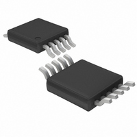
LTC2431CMS#TR Linear Technology, LTC2431CMS#TR Datasheet - Page 22

LTC2431CMS#TR
Manufacturer Part Number
LTC2431CMS#TR
Description
IC ADC 20BIT DIFFINPUT/REF10MSOP
Manufacturer
Linear Technology
Datasheet
1.LTC2431CMSPBF.pdf
(40 pages)
Specifications of LTC2431CMS#TR
Number Of Bits
20
Sampling Rate (per Second)
7.5
Data Interface
MICROWIRE™, Serial, SPI™
Number Of Converters
2
Power Dissipation (max)
1mW
Voltage Supply Source
Single Supply
Operating Temperature
0°C ~ 70°C
Mounting Type
Surface Mount
Package / Case
10-TFSOP, 10-MSOP (0.118", 3.00mm Width)
Lead Free Status / RoHS Status
Contains lead / RoHS non-compliant
Other names
LTC2431CMSTR
Available stocks
Company
Part Number
Manufacturer
Quantity
Price
APPLICATIO S I FOR ATIO
LTC2430/LTC2431
between the F
nals. When the F
converter, substantial AC current is flowing in the loop
formed by the F
ground return path. Thus, perturbation signals may be
inductively coupled into the converter input and/or refer-
ence. In this situation, the user must reduce to a minimum
the loop area for the F
the differential input and reference connections.
Driving the Input and Reference
The input and reference pins of the converter (LTC2430 or
LTC2431) are directly connected to a network of sampling
capacitors. Depending upon the relation between the dif-
ferential input voltage and the differential reference volt-
age, these capacitors are switching between these four
pins transfering small amounts of charge in the process.
A simplified equivalent circuit is shown in Figure 11.
For a simple approximation, the source impedance R
driving an analog input pin (IN
considered to form, together with R
Figure 11), a first order passive network with a time
constant = (R
22
O
SWITCHING FREQUENCY
f
f
O
SW
SW
V
V
I
V
I
S
V
signal trace and the input/reference sig-
I
REF
REF
REF
REF
I
connection trace, the termination and the
IN
IN
IN
IN
= 76800Hz INTERNAL OSCILLATOR (F
= 0.5 • f
O
+ R
+
+
–
–
+
+
–
–
signal is parallel terminated near the
U
SW
V
V
O
EOSC
CC
CC
signal as well as the loop area for
) • C
V
V
EXTERNAL OSCILLATOR
U
I
I
I
I
LEAK
LEAK
LEAK
LEAK
CC
CC
EQ
+
I
I
I
I
LEAK
LEAK
LEAK
LEAK
, IN
. The converter is able to
Figure 11. LTC2430/LTC2431 Equivalent Analog Input Circuit
–
R
R
R
R
W
, REF
SW
SW
SW
SW
20k
20k
20k
20k
(TYP)
(TYP)
(TYP)
(TYP)
SW
+
O
or REF
= LOW OR HIGH)
and C
U
2431 F11
–
EQ
) can be
(see
C
6pF
(TYP)
EQ
S
sample the input signal with better than 1ppm accuracy if
the sampling period is at least 14 times greater than the
input circuit time constant . The sampling process on the
four input analog pins is quasi-independent so each time
constant should be considered by itself and, under worst-
case circumstances, the errors may add.
When using the internal oscillator (F
LTC2430/LTC2431’s front-end switched-capacitor net-
work is clocked at 76800Hz corresponding to a 13 s
sampling period. Thus, for settling errors of less than
1ppm, the driving source impedance should be chosen
such that
of frequency f
and, for a settling error of less than 1ppm,
Input Current
If complete settling occurs on the input, conversion re-
sults will be unaffected by the dynamic input current. An
incomplete settling of the input signal sampling process
may result in gain and offset errors, but it will not degrade
the INL performance of the converter. Figure 11 shows the
mathematical expressions for the average bias currents
flowing through the IN
I IN
I IN
I REF
I REF
WHERE
R
R
R
V
V
V
V
REF
REFCM
IN
INCM
EQ
EQ
EQ
IN
AVG
AVG
43 2
52 0
REF
6 66 10
AVG
: :
AVG
.
.
.
IN
M
M
REF
IN
V
IN
1 5
V
2
REF
.
IN
INTERNAL OSCILLATOR
INTERNAL OSCILLATOR
1 5
IN
12
.
2
13 s/14 = 920ns. When an external oscillator
V
0 5
REF
EOSC
INCM
V
0 5
.
V
/
REF
.
INCM
V
f
EOSC
REF
R
0 5
R
0 5
.
EQ
EQ
.
V
V
EXTERNAL OSCILLATOR
is used, the sampling period is 2/f
REFCM
INCM
V
V
R
REFCM
INCM
R
EQ
EQ
V
+
REFCM
V
REFCM
and IN
60
50
Hz Notch F
Hz Notch F
V
REF
V
REF
V
–
IN
2
V
R
IN
pins as a result of the
2
EQ
R
O
O
O
EQ
= LOW or HIGH), the
LOW
HIGH
0.14/f
EOSC
EOSC
24301f
.


