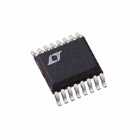
LTC2435-1IGN Linear Technology, LTC2435-1IGN Datasheet - Page 30

LTC2435-1IGN
Manufacturer Part Number
LTC2435-1IGN
Description
IC CONV A/D 20BIT DIFF 16-SSOP
Manufacturer
Linear Technology
Datasheet
1.LTC2435-1CGN.pdf
(40 pages)
Specifications of LTC2435-1IGN
Number Of Bits
20
Sampling Rate (per Second)
13.75
Data Interface
MICROWIRE™, Serial, SPI™
Number Of Converters
2
Power Dissipation (max)
1mW
Voltage Supply Source
Single Supply
Operating Temperature
-40°C ~ 85°C
Mounting Type
Surface Mount
Package / Case
16-SSOP (0.150", 3.90mm Width)
Lead Free Status / RoHS Status
Contains lead / RoHS non-compliant
Available stocks
Company
Part Number
Manufacturer
Quantity
Price
Company:
Part Number:
LTC2435-1IGN
Manufacturer:
LT
Quantity:
10 000
LTC2435/LTC2435-1
APPLICATIO S I FOR ATIO
Output Data Rate
When using its internal oscillator, the LTC2435 can pro-
duce up to 15 readings per second with a notch frequency
of 60Hz (F
notch frequency of 50Hz (F
can produce up to 13.6 readings per second with F
LOW. The actual output data rate will depend upon the
length of the sleep and data output phases which are
controlled by the user and which can be made insignifi-
cantly short. When operated with an external conversion
clock (F
LTC2435-1 output data rate can be increased as desired.
The duration of the conversion phase is 10278/f
f
oscillator is used and the notch is set at 60Hz. There is no
significant difference in the LTC2435/LTC2435-1 perfor-
mance between these two operation modes.
An increase in f
translate into a proportional increase in the maximum
output data rate. This substantial advantage is nevertheless
accompanied by three potential effects, which must be
carefully considered.
First, a change in f
in the internal notch position and in a reduction of the
converter differential mode rejection at the power line
frequency. In many applications, the subsequent perfor-
mance degradation can be substantially reduced by rely-
ing upon the LTC2435/LTC2435-1’s exceptional common
mode rejection and by carefully eliminating common
mode to differential mode conversion sources in the input
circuit. The user should avoid single-ended input filters
and should maintain a very high degree of matching and
symmetry in the circuits driving the IN
Second, the increase in clock frequency will increase
proportionally the amount of sampling charge transferred
through the input and the reference pins. If large external
input and/or reference capacitors (C
previous section provides formulae for evaluating the
effect of the source resistance upon the converter perfor-
mance for any value of f
or reference capacitors (C
the external source resistance upon the LTC2435/
LTC2435-1 typical performance can be inferred from
Figures 16, 17, 21 and 22 in which the horizontal axis is
scaled by 153600/f
30
EOSC
= 153600Hz, the converter behaves as if the internal
O
connected to an external oscillator), the LTC2435/
O
= LOW) and 12.5 readings per second with a
EOSC
EOSC
EOSC
U
over the nominal 153600Hz will
will result in a proportional change
.
EOSC
IN
U
O
, C
. If small external input and/
= HIGH) and the LTC2435-1
REF
) are used, the effect of
IN
W
, C
+
REF
and IN
) are used, the
–
U
pins.
EOSC
O
. If
=
Third, the internal analog circuits are optimized for normal
operation; therefore an increase in the frequency of the
external oscillator will start to decrease the effectiveness
of the internal analog circuits. This will result in a progres-
sive degradation in the converter accuracy and linearity.
Typical measured performance curves for output data rates
up to 200 readings per second are shown in Figures 26 to
33. The degradation becomes more obvious above output
data rate of 150Hz, which corresponds to an external os-
cillator of 1.536MHz. In order to obtain the highest possible
level of accuracy from this converter at output data rates
above 150 readings per second, the user is advised to
maximize the power supply voltage used and to limit the
maximum ambient operating temperature. In certain cir-
cumstances, a reduction of the differential reference volt-
age may be beneficial.
Figure 26. Offset Error vs Output Data Rate and Temperature
Figure 27. + FS Error vs Output Data Rate and Temperature
–300
–310
–320
–330
–340
–350
–300
–320
–340
–360
–380
–400
–420
–440
–460
–480
–500
0
0
V
V
F
V
V
V
F
O
INCM
CC
O
INCM
CC
IN
20 40 60 80 100 120 140 160 180 200
20
= EXT OSC
OUTPUT DATA RATE (READINGS/SEC)
= EXT OSC
OUTPUT DATA RATE (READINGS/SEC)
= V
= 0V
= V
= V
= V
40
REF
REF
REFCM
REFCM
= 5V
60 80 100
= 5V
T
A
= 25°C
T
120 140 160 180 200
A
= 85°C
T
A
T
A
= 25°C
= 85°C
2435 F27
2435 F26
24351fb


