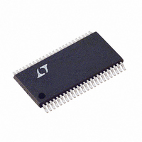
LTC1852IFW#PBF Linear Technology, LTC1852IFW#PBF Datasheet - Page 11

LTC1852IFW#PBF
Manufacturer Part Number
LTC1852IFW#PBF
Description
IC A/D CONV 8CH 10BIT 48-TSSOP
Manufacturer
Linear Technology
Datasheet
1.LTC1853CFWPBF.pdf
(24 pages)
Specifications of LTC1852IFW#PBF
Number Of Bits
10
Sampling Rate (per Second)
400k
Data Interface
Parallel
Number Of Converters
1
Power Dissipation (max)
15mW
Voltage Supply Source
Single Supply
Operating Temperature
-40°C ~ 85°C
Mounting Type
Surface Mount
Package / Case
48-TFSOP (0.240", 6.10mm Width)
Lead Free Status / RoHS Status
Lead free / RoHS Compliant
Available stocks
Company
Part Number
Manufacturer
Quantity
Price
APPLICATIONS INFORMATION
If two pure sine waves of frequencies fa and fb are applied
to the ADC input, nonlinearities in the ADC transfer function
can create distortion products at the sum and difference
frequencies of mfa ± nfb, where m and n = 0, 1, 2, 3, etc.
For example, the 2nd order IMD terms include (fa ± fb).
If the two input sine waves are equal in magnitude, the
value (in decibels) of the 2nd order IMD products can be
expressed by the following formula:
Peak Harmonic or Spurious Noise
The peak harmonic or spurious noise is the largest spectral
component excluding the input signal and DC. This value
is expressed in decibels relative to the RMS value of a
full-scale input signal.
Full-Power and Full-Linear Bandwidth
The full-power bandwidth is that input frequency at which
the amplitude of the reconstructed fundamental is reduced
by 3dB for a full-scale input signal.
The full-linear bandwidth is the input frequency at which
the S/(N + D) has dropped to 68dB for the LTC1853 (11
effective bits) or 56dB for the LTC1852 (9 effective bits).
The LTC1852/LTC1853 have been designed to optimize
input bandwidth, allowing the ADC to undersample input
signals with frequencies above the converter’s Nyquist fre-
quency. The noise fl oor stays very low at high frequencies;
S/(N + D) becomes dominated by distortion at frequencies
far beyond Nyquist.
ANALOG INPUT MULTIPLEXER
The analog input multiplexer is controlled using the
single-ended/differential pin (DIFF), three MUX address
pins (A2, A1, A0), the unipolar/bipolar pin (UNI/BIP) and
the gain select pin (PGA). The single-ended/differential
pin (DIFF) allows the user to confi gure the MUX as eight
single-ended channels relative to the analog input com-
mon pin (COM) when DIFF is low or as four differential
pairs (CH0 and CH1, CH2 and CH3, CH4 and CH5, CH6
and CH7) when DIFF is high. The channels (and polarity in
the differential case) are selected using the MUX address
IMD fa ± fb
(
)
= 20Log
Amplitude at fa ± fb
Amplitude at fa
(
)
inputs as shown in Table 1. Unused inputs (including
the COM in the differential case) should be grounded to
prevent noise coupling.
Table 1. Multiplexer Address Table
DIFF A2
DIFF A2
*Not used in differential mode. Connect to AGND.
In addition to selecting the MUX channel, the LTC1852/
LTC1853 also allows the user to select between two gains
and unipolar or bipolar inputs for a total of four input spans.
PGA high selects a gain of 1 (the input span is equal to the
voltage on REFCOMP). PGA low selects a gain of 2 where
the input span is equal to half of the voltage on REFCOMP .
UNI/BIP low selects a unipolar input span, UNI/BIP high
selects a bipolar input span. Table 2 summarizes the pos-
sible input spans.
Table 2. Input Span Table
0
0
0
0
0
0
0
0
1
1
1
1
1
1
1
1
UNI/BIP
MUX ADDRESS
MUX ADDRESS
0
0
1
1
0
0
0
0
1
1
1
1
0
0
0
0
1
1
1
1
A1
A1
0
0
1
1
0
0
1
1
0
0
1
1
0
0
1
1
PGA
0
1
0
1
A0 CH0 CH1 CH2 CH3 CH4 CH5 CH6 CH7 COM
A0 CH0 CH1 CH2 CH3 CH4 CH5 CH6 CH7 COM
0
1
0
1
0
1
0
1
0
1
0
1
0
1
0
1
+
+
–
LTC1852/LTC1853
0 – REFCOMP/2
0 – REFCOMP
± REFCOMP/4
SINGLE-ENDED CHANNEL SELECTION
±REFCOMP/2
DIFFERENTIAL CHANNEL SELECTION
+
–
+
+
+
–
+
–
+
INPUT SPAN
+
+
–
REFCOMP = 4.096V
+
+
–
0 – 2.048V
0 – 4.096V
±1.024V
±2.048V
+
+
–
11
+
+
–
18523fa
–
–
–
–
–
–
–
–
*
*
*
*
*
*
*
*


