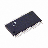
LTC1852IFW#PBF Linear Technology, LTC1852IFW#PBF Datasheet

LTC1852IFW#PBF
Specifications of LTC1852IFW#PBF
Available stocks
Related parts for LTC1852IFW#PBF
LTC1852IFW#PBF Summary of contents
Page 1
... The digital outputs are pow- ered from a separate supply allowing for easy interface to 3V digital logic. Typical power consumption is 10mW at 400ksps from a single 5V supply and 3mW at 250ksps from a single 3V supply. , LT, LTC and LTM are registered trademarks of Linear Technology Corporation. M1 SHDN CS CONVST ...
Page 2
... JMAX JA ORDER INFORMATION LEAD FREE FINISH TAPE AND REEL LTC1852CFW#PBF LTC1852CFW#TRPBF LTC1852IFW#PBF LTC1852IFW#TRPBF LTC1853CFW#PBF LTC1853CFW#TRPBF LTC1853IFW#PBF LTC1853IFW#TRPBF Consult LTC Marketing for parts specifi ed with wider operating temperature ranges. Consult LTC Marketing for information on non-standard lead based fi nish parts. ...
Page 3
CONVERTER CHARACTERISTICS temperature range, otherwise specifi cations are at T PARAMETER CONDITIONS Resolution (No Missing Codes) Integral Linearity Error (Note 7) Differential Linearity Error Offset Error (Bipolar and Unipolar) (Note 8) Gain = 1 (PGA = 1) REFCOMP ≥ 2V ...
Page 4
LTC1852/LTC1853 INTERNAL REFERENCE PARAMETER REFOUT Output Voltage REFOUT Output Temperature Coeffi cient REFOUT Line Regulation Reference Buffer Gain REFCOMP Output Voltage REFCOMP Impedance DIGITAL INPUTS AND DIGITAL OUTPUTS operating temperature range, otherwise specifi cations are at T SYMBOL PARAMETER V ...
Page 5
POWER REQUIREMENTS range, otherwise specifi cations are SYMBOL PARAMETER V Analog Positive Supply Voltage DD OV Output Positive Supply Voltage DD I Positive Supply Current DD P Power Dissipation DISS I Power Down Positive Supply Current DDPD ...
Page 6
LTC1852/LTC1853 TIMING CHARACTERISTICS range, otherwise specifi cations are SYMBOL PARAMETER CONVST High Time Latch Setup Time 14 t Latch Hold Time 15 WR Low Time High Time ...
Page 7
PIN FUNCTIONS CH0 to CH7 (Pins 1 to 8): Analog Input Pins. Input pins can be used single ended relative to the analog input common pin or differentially in pairs (CH0 and CH1, CH2 and CH3, CH4 and CH5, CH6 ...
Page 8
LTC1852/LTC1853 PIN FUNCTIONS D9/S0 (Pin 23, LTC1853): Three-State Digital Data Outputs. Active when RD is low. Following a conversion, bit 9 of the present conversion is available on this pin. In Readback mode, the end of sequence bit of the ...
Page 9
PIN FUNCTIONS PIN NAME DESCRIPTION CH0 to CH7 Analog Inputs 9 COM Analog Input Common Pin 10 REFOUT 2.5V Reference Output 11 REFIN Reference Buffer Input 12 REFCOMP Reference Buffer Output 13 GND Ground 14 V Positive ...
Page 10
LTC1852/LTC1853 APPLICATIONS INFORMATION The LTC1852/LTC1853 are complete and very fl exible data acquisition systems. They consist of a 10-bit/12-bit, 400ksps capacitive successive approximation A/D con- verter with a wideband sample-and-hold, a confi gurable 8-channel analog input multiplexer, an internal reference ...
Page 11
APPLICATIONS INFORMATION If two pure sine waves of frequencies fa and fb are applied to the ADC input, nonlinearities in the ADC transfer function can create distortion products at the sum and difference frequencies of mfa ± nfb, where m ...
Page 12
... Feedback Amplifi ers. Single 3V to ±15V supplies. 4.3mA supply current per amplifi er. Low distortion. LT1806/LT1807: Single and Dual 325MHz Rail-to-Rail Voltage Feedback Amplifi er. Single 3V to ± 5V supplies. 13mA supply current. Lowest distortion. LinearView is a trademark of Linear Technology Corporation. ™ 18523fa ...
Page 13
APPLICATIONS INFORMATION LT1809/LT1810: Single and Dual 180MHz Rail-to-Rail Voltage Feedback Amplifi er. Single 3V to ±15V supplies. 20mA supply current. Lowest distortion. LT1812/LT1813: Single and Dual 100MHz Voltage Feed- back Amplifi er. Single 5V to ±5V supplies. 3.6mA supply current. ...
Page 14
LTC1852/LTC1853 APPLICATIONS INFORMATION adjusted until the output code fl ickers between 1111 1111 1110 and 1111 1111 1111 for the LTC1853 and between 11 1111 1110 and 11 1111 1111 for the LTC1852. For bipolar inputs, an input voltage of ...
Page 15
APPLICATIONS INFORMATION BOARD LAYOUT AND BYPASSING To obtain the best performance from the LTC1852/LTC1853, a printed circuit board with ground plane is required. The ground plane under the ADC area should be as free of breaks and holes as possible, ...
Page 16
LTC1852/LTC1853 APPLICATIONS INFORMATION CONVST Figure CONVST and RD Setup Timing Power Shutdown The LTC1852/LTC1853 provide two power shutdown modes, Nap and Sleep, to save power during inactive periods. The Nap mode ...
Page 17
APPLICATIONS INFORMATION t 13 CONVST BUSY DATA Figure 6. Mode 1b CONVST Starts a Conversion CONVST t 6 BUSY RD DATA Figure 7. Mode 2 CONVST Starts a Conversion. Data is Read by ...
Page 18
LTC1852/LTC1853 APPLICATIONS INFORMATION appear on the data outputs; BUSY goes high releasing the processor, and the processor takes CONVST) back high and reads the new conversion data. In ROM mode, the processor takes CONVST) ...
Page 19
APPLICATIONS INFORMATION The sequencer is accessed by taking the M1 mode pin high. With M1 high, the sequencer memory is accessed by taking the M0 mode pin low. This will cause BUSY to go low, disabling conversions during the programming ...
Page 20
LTC1852/LTC1853 APPLICATIONS INFORMATION 20 18523fa ...
Page 21
APPLICATIONS INFORMATION LTC1852/LTC1853 18523fa 21 ...
Page 22
LTC1852/LTC1853 TYPICAL APPLICATIONS LTC1853 Hardwired for 8-Channel Single-Ended Scan with Unipolar 0V to 4.096V Operation V 1 CH0 2 CH1 3 CH2 4 CH3 INPUT CONFIGURATION: ALL 8 CHANNELS 8-CHANNEL 5 CH4 SINGLE ENDED MULTIPLEXER TO COM 6 CH5 CH0–CH7: ...
Page 23
... DIMENSIONS DO NOT INCLUDE INTERLEAD FLASH. INTERLEAD FLASH SHALL NOT EXCEED .254mm (.010") PER SIDE Information furnished by Linear Technology Corporation is believed to be accurate and reliable. However, no responsibility is assumed for its use. Linear Technology Corporation makes no representation that the interconnection of its circuits as described herein will not infringe on existing patent rights. ...
Page 24
... IDT7202LA15 13 8-BIT × 1k DATA BUS READ_HIGH_FIFO HIGH_FIFO_EMPTY HIGH_FIFO_HALF_FULL 23 RT HIGH BYTE_FIFO_RETRANSMIT XI GND 7 14 HIGH_FIFO_FULL_FLAG LOW_FIFO_FULL_FLAG FIFO_RESET 0.1μ IDT7202LA15 × READ_LOW_FIFO LOW_FIFO_EMPTY LOW_FIFO_HALF_FULL 23 RT LOW BYTE_FIFO_RETRANSMIT XI GND 7 14 18523 TA03 18523fa LT 0108 REV A • PRINTED IN USA © LINEAR TECHNOLOGY CORPORATION 2001 ...


